This content is translated with AI. Please refer to the original Traditional Chinese version (zh-TW) for accuracy.
Last time, we implemented UART input and output. This time, let’s take on another interface included on the board: HDMI. With this implementation, we will have video output available. However, HDMI is a level more difficult than UART, so this time I directly modified the example code of icesugar-pro. For the TMDS part, I referred to an encoder available online.
HDMI protocol
High Definition Multimedia Interface, HDMI (High-definition Multimedia Interface) is a video interface that is quite widely used. The board uses the HDMI pin A 17 pins . However, if you look closely, you can see it only connects 8 pins plus the ground, which are:
- 1,3 Data 2+/- blue
- 4,6 Data 1+/- green
- 7,9 Data 0+/- red
- 10,12 Data Clock +/-
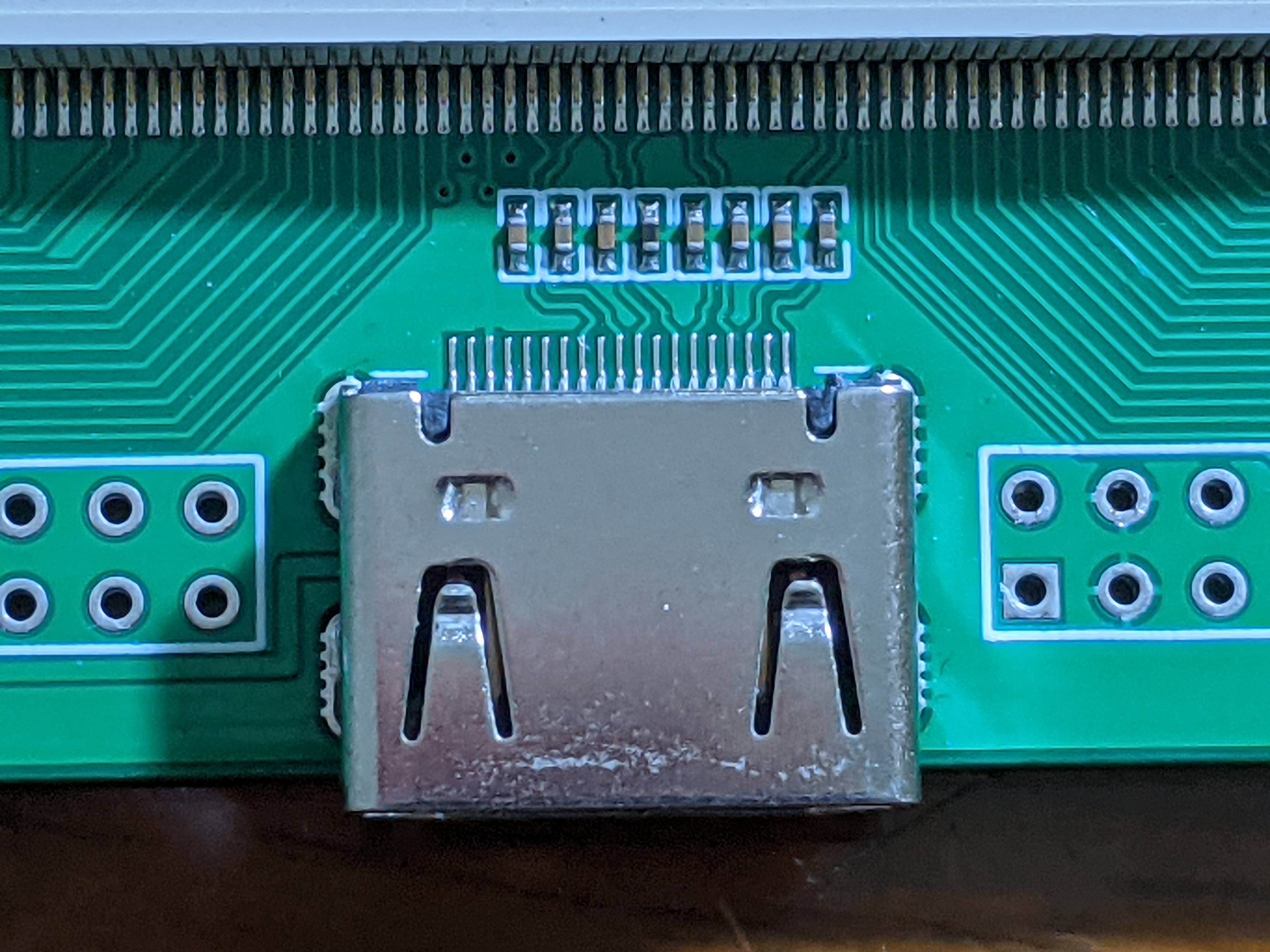
HDMI signals use differential transmission, which achieves a higher rate compared to UART’s single-ended transmission. Related articles can be seen in this article . Since it is not connected, we can’t play with the I2C from the later pins of HDMI, which should be used for audio, so we are not concerned with it anyway. Additionally, for reasons unknown, the HDMI pinout cannot be found in its schematic or pictures. We can only follow the example lpf file:
LOCATE COMP "hdmi_dp[0]" SITE "G1"; # Blue +
LOCATE COMP "hdmi_dn[0]" SITE "F1"; # Blue -
LOCATE COMP "hdmi_dp[1]" SITE "J1"; # Green +
LOCATE COMP "hdmi_dn[1]" SITE "H2"; # Green -
LOCATE COMP "hdmi_dp[2]" SITE "L1"; # Red +
LOCATE COMP "hdmi_dn[2]" SITE "K2"; # Red -
LOCATE COMP "hdmi_dp[3]" SITE "E2"; # Clock +
LOCATE COMP "hdmi_dn[3]" SITE "D3"; # Clock -

IOBUF PORT "hdmi_dp[0]" IO_TYPE=LVCMOS33 DRIVE=4;
IOBUF PORT "hdmi_dn[0]" IO_TYPE=LVCMOS33 DRIVE=4;
IOBUF PORT "hdmi_dp[1]" IO_TYPE=LVCMOS33 DRIVE=4;
IOBUF PORT "hdmi_dn[1]" IO_TYPE=LVCMOS33 DRIVE=4;
IOBUF PORT "hdmi_dp[2]" IO_TYPE=LVCMOS33 DRIVE=4;
IOBUF PORT "hdmi_dn[2]" IO_TYPE=LVCMOS33 DRIVE=4;
IOBUF PORT "hdmi_dp[3]" IO_TYPE=LVCMOS33 DRIVE=4;
IOBUF PORT "hdmi_dn[3]" IO_TYPE=LVCMOS33 DRIVE=4;
PLL
Since HDMI operates in this way, using 24-bit color per pixel on the screen, with each RGB component occupying one byte. During transmission, it utilizes 8b/10b encoding , adding two bits to each byte of data. Using TMDS Transition-minimized Differential Signaling , it is padded to 10 bits, and then transmitted through the differential signal mentioned above.
The FPGA operates at 25MHz, and the serial port data rate will be 250 MHz, requiring a fast clock on the FPGA, which necessitates using a PLL. Fortunately, the FPGA LFE5U-25F-6BG256C used in icesugar-pro does provide a PLL. By looking up the model and datasheet on Google, you can find the datasheet provided by Lattice. Additionally, another datasheet dedicated to PLLs can be found in the ECP5 and ECP5-5G sysCLOCK PLL/DLL Design and Usage Guide. Since these are links to pdfs, I will not attach them here.
If you use Lattice’s integrated development environment Lattice Diamond , it provides a graphical PLL configuration tool that should generate usable verilog code directly, but since we don’t have a license, we have to do it manually.
Manual steps are as follows; first, check the PLL datasheet, starting in Chapter 18, which provides a complete introduction to PLL architecture:
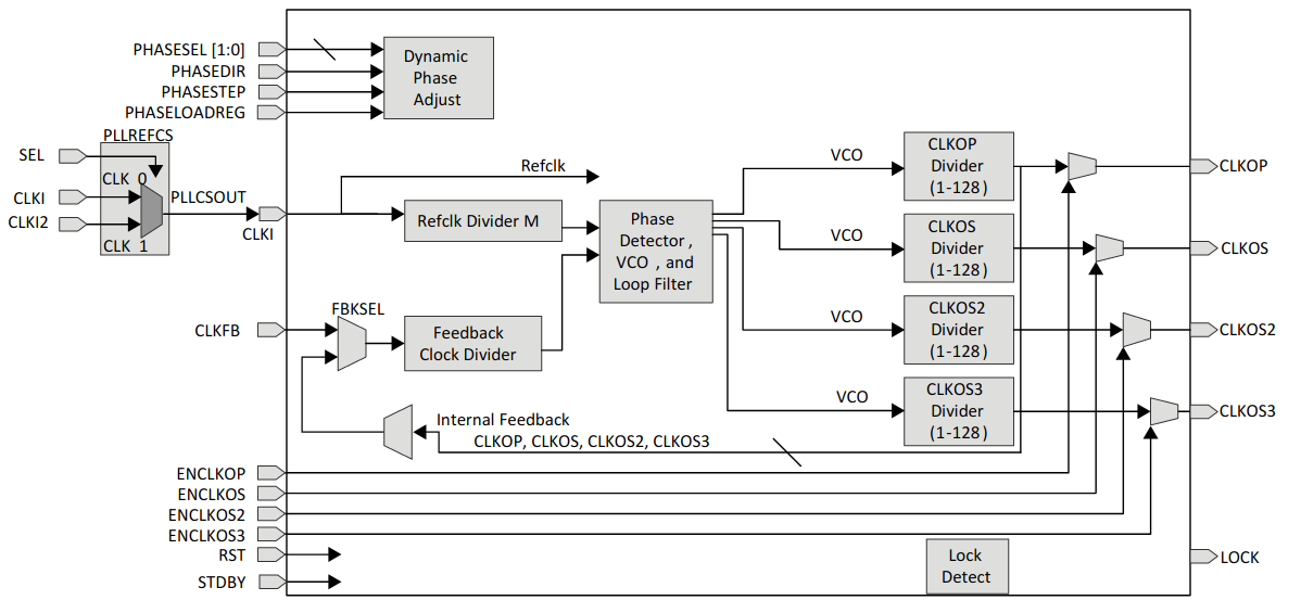
The operation of the PLL is as follows: First, you have an input clock, then provide a feedback clock, both entering the VCO in the middle. The VCO adjusts the output clock frequency until the input and feedback phases are locked; how to achieve this is a specialized subject that likely requires taking a phase-locked loop course by Abyss .
Table 18.1 provides the list of inputs and outputs for the verilog module, and some parameters need to be set according to the list in Table 18.6. Our goal is to generate 250 MHz output from 25 MHz input, selecting the primary output CLKOP to generate 250 MHz; CLKOS generates 25 MHz clock as feedback clock, and all other clocks are turned off.
Here, for some reason not stated in the PLL document but instead in LFE5U-25F-6BG256C’s document, the recommended VCO usage range is 400-800 MHz. Therefore, we set the VCO frequency to 500 MHz, with CLKOP and CLKOS divided by 2 and 20 respectively.
Below is the clock.sv file I wrote:
module clock
(
  input clkin_25MHz,
  output clk_25MHz,
  output clk_250MHz,
  output locked
);

(* ICP_CURRENT="9" *) (* LPF_RESISTOR="8" *) (* MFG_ENABLE_FILTEROPAMP="1" *) (* MFG_GMCREF_SEL="2" *)
EHXPLLL
#(
  .CLKOS_FPHASE(0),
  .CLKOP_FPHASE(0),
  .CLKOS_CPHASE(2),
  .CLKOP_CPHASE(20),
  .CLKOS_ENABLE("ENABLED"),
  .CLKOP_ENABLE("ENABLED"),
  .CLKI_DIV(1),
  .CLKOP_DIV(2),
  .CLKOS_DIV(20),
  .CLKFB_DIV(1),
  .FEEDBK_PATH("CLKOS")
)
pll_i
(
  .CLKI(clkin_25MHz),
  .CLKFB(clk_25MHz),
  .CLKOP(clk_250MHz),
  .CLKOS(clk_25MHz),
  .CLKOS2(),
  .CLKOS3(),
  .RST(1'b0),
  .STDBY(1'b0),
  .PHASESEL0(1'b0),
  .PHASESEL1(1'b0),
  .PHASEDIR(1'b0),
  .PHASESTEP(1'b0),
  .PLLWAKESYNC(1'b0),
  .ENCLKOP(1'b0),
  .ENCLKOS(1'b0),
  .ENCLKOS2(),
  .ENCLKOS3(),
  .LOCK(locked),
  .INTLOCK()
);
endmodule
I am not sure what the ICP_CURRENT at the top does, but after reading the FAQ , it is related to some LPF parameter settings and will be generated by the tool automatically. It does not affect the final result whether I keep it or not. As you can see, I only kept the settings for CLKOP and CLKOS, dividing CLKOP by 2 into 250 MHz and CLKOS by 20 to 25 MHz and feeding back to CLKFB. Using FPHASE and CPHASE, you can adjust the phase of the output signal, but we do not set the phase here.
HDMI
module hdmi(
  input clk_tmds,
  input clk_pixel,
  input rst,
  input [7:0] i_red, i_green, i_blue,
  output logic o_enable,
  output logic o_newline,
  output logic o_newframe,
  output logic o_red,
  output logic o_green,
  output logic o_blue);
The HDMI module interface is as follows:
- clk_tmds/clk_pixel 250 MHz and 25 MHz clocks
- i_red/green/blue RGB data each a byte
- o_red/o_green/o_blue bits sent to the serial line
- o_enable, o_newline, o_newline informing the data source of the line currently being displayed, they are not actually sent to the screen.
parameter WIDTH = 640;
parameter HEIGHT = 480;
parameter VWIDTH = 800;
parameter VHEIGHT = 525;

logic [9:0] CounterX, CounterY;

// update counterX and counterY
always_ff @(posedge clk_pixel or negedge rst) begin
  if (!rst) begin
    CounterX <= 0;
  end
  else begin
    if (CounterX == VWIDTH-1) begin
      CounterY <= (CounterY == VHEIGHT-1) ? 0 : CounterY+1;
    end
  end
end

always_ff @(posedge clk_pixel or negedge rst) begin
  if (!rst) begin
    CounterY <= 0;
  end
  else begin
    if (CounterX == VWIDTH-1) begin
      CounterY <= (CounterY == VHEIGHT-1) ? 0 : CounterY+1;
    end
  end
end
By calculating counterX and counterY via clk_pixel, we can determine which pixel is currently being processed.
logic hSync, vSync, DrawArea;

// Signal end of line, end of frame
assign o_newline  = (CounterX == WIDTH-1);
assign o_newframe = (CounterX == WIDTH-1) && (CounterY == HEIGHT-1);
assign DrawArea   = (CounterX < WIDTH) && (CounterY < HEIGHT);
assign o_enable   = rst & DrawArea;
assign hSync = (CounterX >= 656) && (CounterX < 752);
assign vSync = (CounterY >= 490) && (CounterY < 492);
This part is just some lines that change according to CounterX and CounterY. The timing of hSync and vSync seems to be set by the HDMI standard
, which dictates that during X=656752 and Y=490492, hSync and vSync settings must be entered. Because of future projects, I am really curious whether the timing of hSync and vSync can be adjusted freely?
logic [9:0] tmds_red, tmds_green, tmds_blue;
logic [9:0] tmds_red_next, tmds_green_next, tmds_blue_next;
TMDS_encoder encode_R(.clk(clk_pixel), .rst(rst), .data(i_red), .control(2'b00),
  .enable(DrawArea), .tmds(tmds_red_next));
TMDS_encoder encode_G(.clk(clk_pixel), .rst(rst), .data(i_green), .control(2'b00),
  .enable(DrawArea), .tmds(tmds_green_next));
TMDS_encoder encode_B(.clk(clk_pixel), .rst(rst), .data(i_blue), .control({vSync,hSync}),
  .enable(DrawArea), .tmds(tmds_blue_next));
Put the red/green/blue byte into TMDS_encoder and encode it into 10-bits signal tmds_*_next.
logic [3:0] tmds_counter=0;
always @(posedge clk_tmds) begin
  if (!rst) begin
    tmds_counter <= 0;
    tmds_red   <= 0;
    tmds_green <= 0;
    tmds_blue  <= 0;
  end else begin
    tmds_counter <= (tmds_counter==4'd9) ? 4'd0 : tmds_counter+4'd1;
    tmds_red   <= (tmds_counter == 4'd9)? tmds_red_next: tmds_red >> 1;
    tmds_green <= (tmds_counter == 4'd9)? tmds_green_next: tmds_green >> 1;
    tmds_blue  <= (tmds_counter == 4'd9)? tmds_blue_next: tmds_blue >> 1;
  end
end

assign o_red   = tmds_red[0];
assign o_green = tmds_green[0];
assign o_blue  = tmds_blue[0];
Every 10 tmds clock cycles, we update the next round of data into tmds_RGB; otherwise, the original data shifts to the right, and o_red/o_green/o_blue sends out the LSB of that data.
TMDS
TMDS is probably the most troublesome part this time, the module declaration:
module TMDS_encoder(
  input clk, // 250 MHz
  input rst,
  input [7:0] data,  // video data (red, green or blue)
  input [1:0] control,  // control data
  input enable,  // enable == 1 ? data : control
  output logic [9:0] tmds
);

typedef enum logic [9:0] {
  CTRL_00 = 10'b1101010100,
  CTRL_01 = 10'b0010101011,
  CTRL_10 = 10'b0101010100,
  CTRL_11 = 10'b1010101011
} control_t;
We need to encode 8 bits of data into 10 bits of tmds. For the control, as called in the hdmi module, control signals h_sync and v_sync will be transmitted on the blue channel. These two signals correspond to the four TMDS control signals written above.
Next, the TMDS process can be divided into the following two steps:
1. XOR/XNOR
In the first step, the data undergoes rolling xor or rolling xnor , choosing either based on which produces fewer 0-1 transitions. Implementation-wise, just count the number of 1s in the 8 bits, and if it is more than 4, it will be xnor. The reason for this is as follows:
| input | operator | output |
|---|---|---|
| 00 | XOR | 00 |
| 00 | XNOR | 01 |
| 01 | XOR | 01 |
| 01 | XNOR | 00 |
| 10 | XOR | 11 |
| 10 | XNOR | 10 |
| 11 | XOR | 10 |
| 11 | XNOR | 11 |
As seen, only when the next bit is 0, XOR’s result does not have a transition, whereas XNOR does. Therefore, the more 1s there are, the fewer transitions there will be with XNOR. If the sequence has an equal number of 0s and 1s, the first bit is checked: if it is 1, it indicates that with the remaining 7 bits, there will be fewer 1s, so XOR should be chosen.
logic [3:0] ones_d;
bit use_xor;
logic [7:0] qm;

function automatic logic [3:0] count_ones(input logic [7:0] bits);
  count_ones = 0;
  int i;
  for (i = 0; i < 8; i = i+1) begin
    count_ones += $bits(count_ones)'(bits[i]);
  end
endfunction

function automatic logic [7:0] rolling_xor(input logic [7:0] bits);
  rolling_xor[0] = bits[0];
  int i;
  for (i = 1; i < 8; i = i+1) begin
    rolling_xor[i] = rolling_xor[i-1] ^ bits[i];
  end
endfunction

function automatic logic [7:0] rolling_xnor(input logic [7:0] bits);
  rolling_xnor[0] = bits[0];
  int i;
  for (i = 1; i < 8; i = i+1) begin
    rolling_xnor[i] = rolling_xnor[i-1] ^~ bits[i];
  end
endfunction

// stage 1: rolling_xor or rolling_xnor the data
assign ones_d = count_ones(data);
assign use_xor = ones_d < 4 || (ones_d == 4 && data[0] == 1'b1);
assign qm = (use_xor)? rolling_xor(data) : rolling_xnor(data);
This uses systemverilog functions and for loops to expand the code;
Though the for loop in yosys is just like C89, where declaration cannot be written inside the for loop, quite useless.
JJL: If it wasn’t this useless, how would companies like S and C make money?
2. Invert
In the second step, TMDS looks at the result of XOR/XNOR and the difference between 0s and 1s, possibly inverting all bits to balance the number of 0s and 1s.
// stage 2: invert bits to compensate diff in 1s or 0s
assign ones_qm = count_ones(qm);
assign diff_qm = (signed'(5'(ones_qm) << 1)) - 5'd8;

always_comb begin
  if (disparity == 0 && ones_qm == 4) begin
    // balanced, set invert_qm to compensate xor bit
    invert_qm = ~use_xor;
  end
  else begin
    invert_qm = (disparity > 0 && ones_qm > 4) || (disparity < 0 && ones_qm < 4);
  end
end
Use XOR 1 / XNOR 0 stored in the 9th bit and invert 1 / non-invert 0 stored in the 10th bit. Finally, place the signal into the output tmds and update the disparity. If not in the display area, send control signals.
always_ff @(posedge clk) begin
  if (enable) begin
    tmds <= {invert_qm, use_xor, invert_qm ? ~qm : qm};
    disparity <= disparity +
      (invert_qm ? -($bits(disparity)'(diff_qm)) : $bits(disparity)'(diff_qm)) +
      (invert_qm ? $bits(disparity)'('sd1) : -($bits(disparity)'('sd1)));
  end
  else begin
    disparity <= 0;
    case (control)
      2'b00: tmds <= CTRL_00;
      2'b01: tmds <= CTRL_01;
      2'b10: tmds <= CTRL_10;
      2'b11: tmds <= CTRL_11;
    endcase
  end
end
Test Pattern
Similar to the example code, using vgatestsrc to generate test screens will display the Test Pattern .
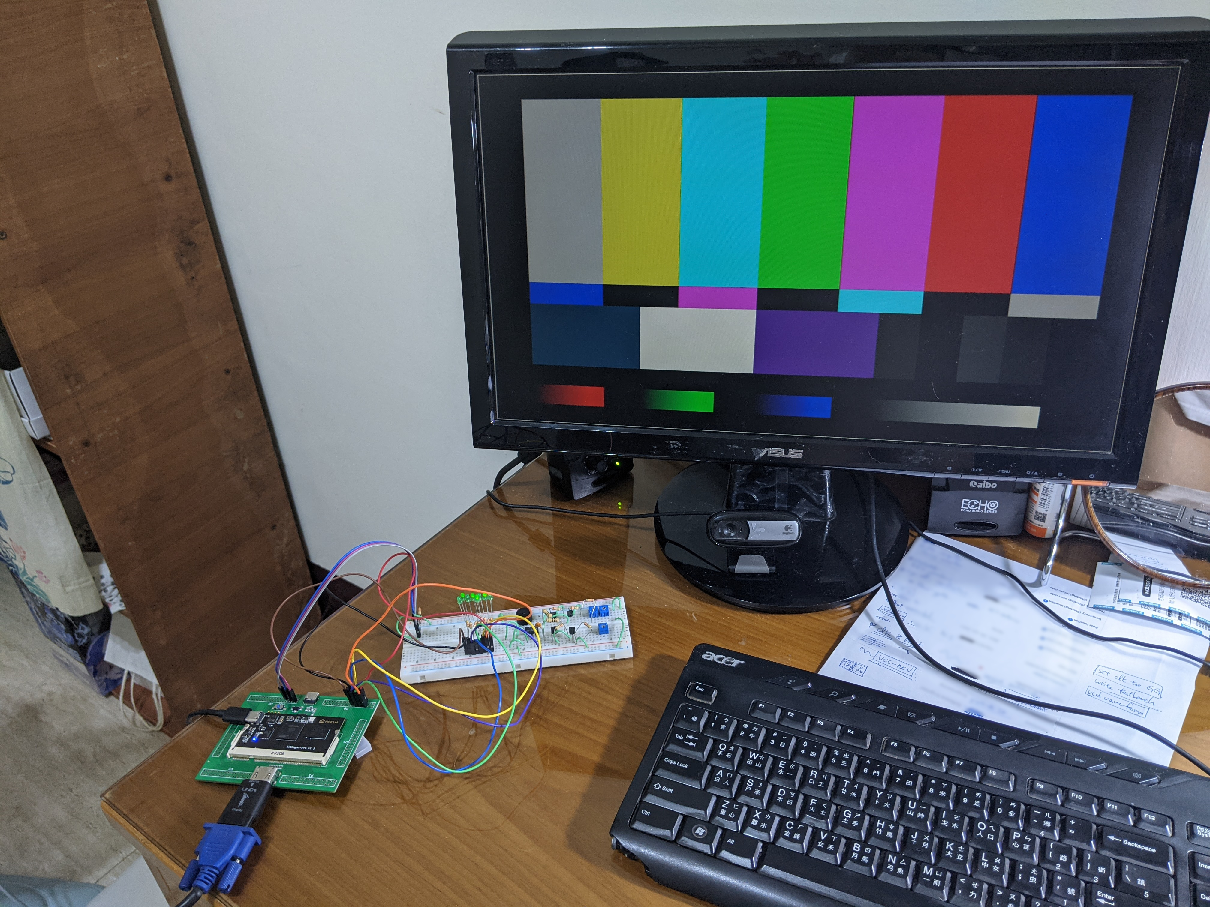
This screen has a somewhat old-fashioned feel.
Conclusion
Whether it’s the UART from the last article or the HDMI in this one, the best way to understand the operation principles of some communication interfaces is to use an FPGA to implement them; just like understanding operating systems’ principles, the best way is to make one yourself, although I haven’t finished mine yet.
With UART and HDMI, we now have a text interface for input/output, and output for displays. The next step might be to test the accompanying SDRAM to see how to access it. I remember my strong classmate Shi Boshen once made a DRAM controller himself; perhaps I should ask him for the code (heh)