This content is translated with AI. Please refer to the original Traditional Chinese version (zh-TW) for accuracy.
In the previous chapter, we mastered the open-source toolchain for FPGA. Next, we can test some of the interfaces of icesugar-pro. First, implementing an FPGA requires input and output, otherwise, it would just be a non-interactive program. The simplest input/output interface would be UART. A UART example is also provided on icesugar-pro’s GitHub, where it continuously outputs “0” to “9” to your computer (note that there is a bug in this code XD). In this article, we will write a UART module with tx and rx.
UART
UART stands for Universal Asynchronous Receiver/Transmitter, or 通用非同步收發傳輸器 in Chinese. You can refer to this article for its principles. The same site also provides VHDL/Verilog UART implementations .
For detailed explanations in Chinese, you can refer to Albert’s notes .
UART is quite simple; communication can be achieved with just one wire. Typical interfaces will have two wires, Tx and Rx, for bi-directional communication. When idle, the communication line remains at a high voltage. This reflects the habits of ancient devices: a high signal indicates normalcy, while a broken wire would appear as open. The entire communication consists of four parts:
- Idle: Maintain a high voltage.
- Start: Transition from 1 to 0 indicates communication start.
- Data 5-9 bits: I was curious about the 5-9 bits description and looked at this post and found that the UART specification dates back to the 1970s when teletype machines were not yet unified. There were 5-bit Baudot codes and 7-bit ASCII (yes, ASCII actually requires only 7 bits), Eventually, the ubiquitous 8-bit byte became the mainstream UART format used today.
- Parity: A configurable parity bit that can be set to odd parity/even parity.
- Stop bit: 1, 1.5, or 2 stop bits, which simply return to high voltage.
This time, we chose the simplest implementation: no parity bit, 1 stop bit, and 8-bit data.
From Verilog to System Verilog
Here’s the story: while writing, I ran into some issues, so I consulted a strong classmate of mine, phoning. He suggested not using Verilog anymore, calling it a thing of the past century. If one cannot embrace next-generation Scala/chisel, at least upgrade to System Verilog. So, I decided to upgrade mentally. After reading some documentation and articles, I made the following changes to Verilog programs:
Logic
In Verilog, variables are divided into wire and reg, where reg originally meant that there was an actual register that stored this value; wire was the result of connecting logic gates. But these can be easily confused in Verilog. System Verilog unified them with logic. My strong classmate johnjohnlin even joked that converting from Verilog to System Verilog was just:
:%s/reg/logic/g
:%s/wire/logic/g
Enum
Because writing Verilog (at least from my experience) often requires writing state machines, you will see it in the UART module implementation. Writing a state machine needs to first pull out the bits representing the state. In Verilog, I might use localparam to define them, but that messes up the code, and the types of each state can’t be unified. System Verilog provides enum to unify state data types, and variables can be declared with enum.
bit/byte/shortint/int/longint
Compared to Verilog, which can only declare certain widths using reg/wire [WIDTH:0], System Verilog offers these types to directly represent data of 1/8/16/32/64 bits. The writing becomes much clearer.
always_ff, always_comb, always_latch
Verilog has only one always keyword, which might synthesize into combinational circuits, flip-flops, latches, etc., due to how it’s written. Even experienced circuit designers might create unintentional results. System Verilog separated always_ff/always_comb/always_latch for these three types of synthesis circuits, allowing more checks to ensure the design matches the result.
Implementation
Reset Signal
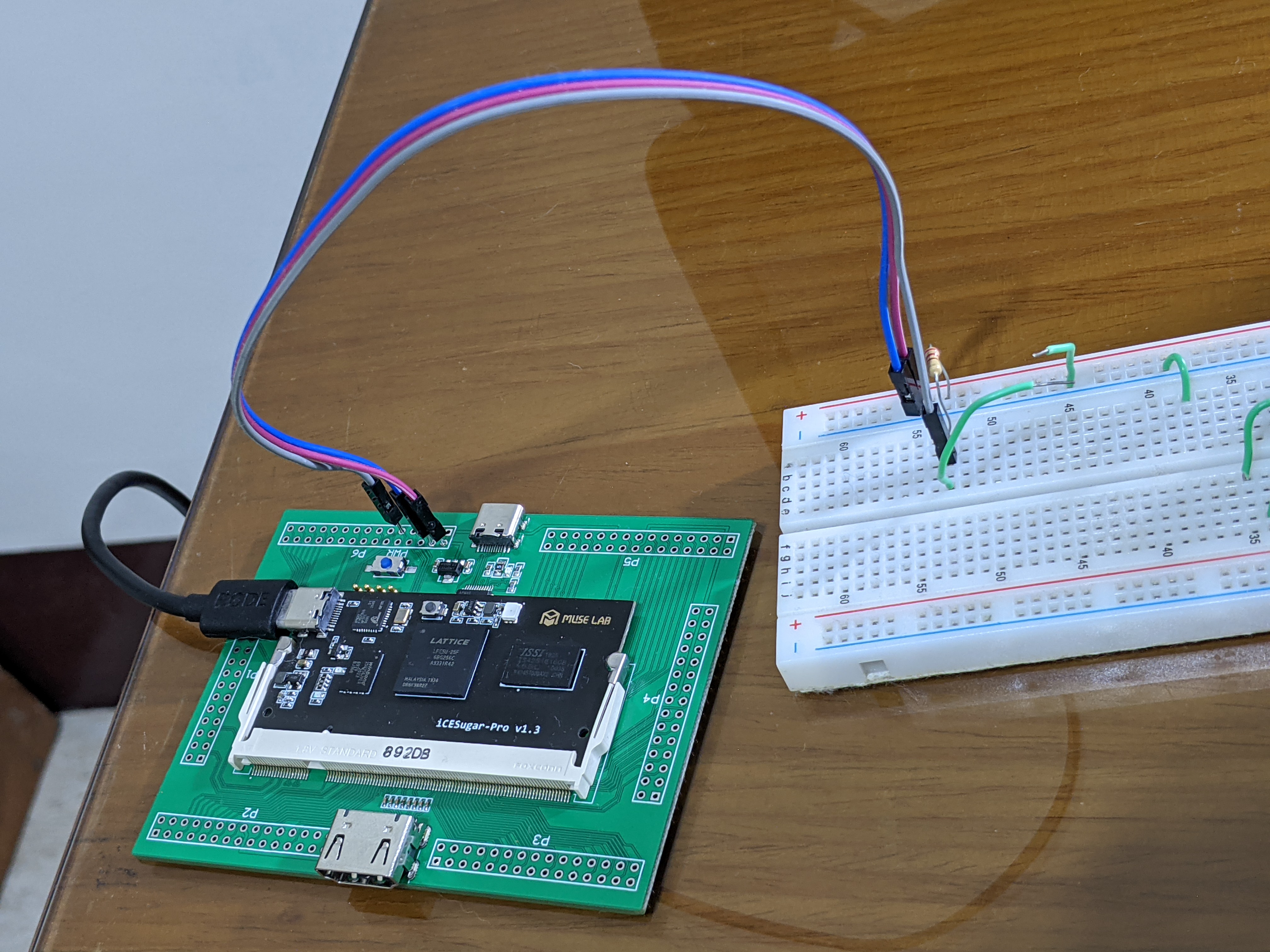
Typically, FPGA requires a reset signal, but our icesugar… doesn’t. It only has a re-program button, which reads the bitstream from flash to program the FPGA. Luckily, there are many GPIOs available, and my wiring is shown in the picture. By connecting 3.3V, GND, and GPIO F14 and letting F14 touch GND by hand, a reset can be achieved. Electronic components bought earlier for nixie tube clock were useful again.
LPF File
Our UART module pins are as follows:
LOCATE COMP "clk" SITE "P6";
IOBUF PORT "clk" IO_TYPE=LVCMOS33;
FREQUENCY PORT "clk" 25 MHZ;

LOCATE COMP "rst" SITE "F14";
IOBUF PORT "rst" IO_TYPE=LVCMOS33;

LOCATE COMP "uart_tx" SITE "B9";
IOBUF PORT "uart_tx" IO_TYPE=LVCMOS33;

LOCATE COMP "uart_rx" SITE "A9";
IOBUF PORT "uart_rx" IO_TYPE=LVCMOS33;
- F14 is a GPIO port; refer to the wiring diagram on GitHub to find the corresponding port.
- B9 is the FPGA’s UART Tx, connected to iCElink’s UART Rx, which connects another UART set through USB to the computer, as seen in the schematic .
- Similarly, A9 connects to iCElink UART Tx.
Module UART Tx
Let’s start with the UART Tx module, interface design:
module uart_tx (
  /* input */
  input clk_baud,
  input rst,
  input [7:0] tx_byte,
  input start_send,

  /* output */
  output logic tx,
  output logic done
);

parameter CLK_PER_BAUD = 1;
localparam CLK_CNT_LIMIT = CLK_PER_BAUD-1;
localparam TX_LENGTH = 10; // start 1'b0, 1 byte, end 1'b1

typedef enum logic {
  STATE_IDLE  = 0,
  STATE_TXING = 1
} State_t;
State_t state = STATE_IDLE, state_next;
logic [9:0] tx_buf;
logic [3:0] tx_idx, tx_idx_next;
int  clk_cnt, clk_cnt_next;
This interface design isn’t much different from Verilog. Data widths for inputs/outputs are still set manually, and byte cannot be used to represent byte input; start_send is for receiving start commands, and done signifies transmission completion; tx connects to the UART tx transmission line.
Parameter module
is something new I learned. Since the FPGA operates at frequencies much higher than the 9.6 kHz baud rate, generating a 9.6 kHz clock for the UART module outside seems unreasonable.
Here, the UART module takes the full-speed clk, and the parameter tells the UART module the clock frequency.
As mentioned above, we use enum to define state_t. What I am not quite satisfied with is that the yosys synthesizer apparently doesn’t perform static checks.
I wrote STATE_TEST = 2 without it uttering a word, though it doesn’t fit. At least it should warn me.
Next is writing a state machine , using a structure I wrote ages ago in the three-block architecture, which seems verbose but is clear in structure.
Feeding the next state into the register’s flip flop, tx_buf is only fed in the instant of IDLE with start_send:
/* update state logic */
always_ff @(posedge clk or negedge rst) begin
  if (!rst) begin
    state   <= STATE_IDLE;
    tx_buf  <= 0;
    tx_cnt  <= 0;
    clk_cnt <= 0;
  end
  else begin
    if (state == STATE_IDLE && start_send) begin
      tx_buf <= {1'b1, tx_byte, 1'b0};
    end
    state   <= state_next;
    tx_cnt  <= tx_idx_next;
    clk_cnt <= clk_cnt_next;
  end
end
The logic circuit part uses System Verilog’s always_comb to generate the next state; Note that we only have two states: IDLE and TXING. This was advised by my strong classmate JJL. The opening 1’b0 and ending 1’b1 are stuffed into the tx_buf being transmitted. tx_idx records the currently sending bit; clk_cnt calculates clk to generate a 9600 kHz timing.
/* next logic for clk_cnt */
always_comb begin
  clk_cnt_next = (state == STATE_IDLE || clk_cnt == CLK_CNT_LIMIT) ? 0 : clk_cnt+1;
end

/* next logic for state */
always_comb begin
  case (state)
    STATE_IDLE: begin
      state_next = (start_send == 1'b1) ? STATE_TXING : state;
    end
    STATE_TXING: begin
      if (clk_cnt == CLK_CNT_LIMIT && tx_idx == TX_LENGTH-1) begin
        state_next = STATE_IDLE;
      end
      else begin
        state_next = state; end
      end
  endcase
end
Output logic part isn’t particularly special.
/* output logic */
assign done = tx_idx == TX_LENGTH - 1;
assign tx = (state == STATE_IDLE) ? 1'b1 : tx_buf[tx_idx];
Module UART Rx
The rx module isn’t much different from tx:
module uart_rx (
  /* input */
  input clk,
  input rst,
  input rx,

  /* output */
  output logic [7:0] rx_byte,
  output logic done
);

parameter CLK_PER_BAUD = 1;
localparam CLK_CNT_LIMIT = CLK_PER_BAUD-1;
localparam SAMPLE_CLK_CNT = CLK_CNT_LIMIT / 2;
localparam RX_LENGTH = 10; // start 1'b0, 1 byte, end 1'b1

typedef enum logic {
  STATE_IDLE  = 0,
  STATE_RXING = 1
} State_t;
State_t state = STATE_IDLE, state_next;
logic [9:0] rx_buf;
logic [3:0] rx_idx, rx_idx_next;
int  clk_cnt, clk_cnt_next;

/* output logic */
assign done = rx_idx == RX_LENGTH - 1;
assign rx_byte = rx_buf[8:1];
The purpose of having SAMPLE_CLK_CNT is to find the midpoint in the 9600 Hz cycle and sample the value on the rx wire at that point; the state machine also uses two states. In STATE_RXING, the initial and ending 1’b0, 1’b1, along with the data are written sequentially into rx_buf, and the output rx_byte takes the middle portion from rx_buf.
/* next logic for clk_cnt */
always_comb begin
  clk_cnt_next = (state == STATE_IDLE || clk_cnt == CLK_CNT_LIMIT) ? 0 : clk_cnt+1;
end

/* next logic for state */
always_comb begin
  case (state)
    STATE_IDLE: begin
      state_next = (rx == 1'b0) ? STATE_RXING : state;
    end
    STATE_RXING: begin
      if (clk_cnt == CLK_CNT_LIMIT && rx_idx == RX_LENGTH-1) begin state_next = STATE_IDLE; end
      else begin state_next = state; end
    end
  endcase
end

/* next logic for rx_idx */
always_comb begin
  if (state == STATE_RXING && rx_idx < RX_LENGTH) begin
    if (clk_cnt == CLK_CNT_LIMIT) begin
      rx_idx_next = rx_idx+1;
    end
    else begin
      rx_idx_next = rx_idx;
    end
  end
  else begin
    rx_idx_next = 0;
  end
end

/* update state logic */
always_ff @(posedge clk or negedge rst) begin
  if (!rst) begin
    state   <= STATE_IDLE;
    rx_buf  <= 0;
    rx_idx  <= 0;
    clk_cnt <= 0;
  end
  else begin
    if (clk_cnt == SAMPLE_CLK_CNT) begin
      rx_buf[rx_idx] <= rx;
    end
    state   <= state_next;
    rx_idx  <= rx_idx_next;
    clk_cnt <= clk_cnt_next;
  end
end
This segment isn’t particularly special; the only difference is in the flip flop feeding register, where at SAMPLE_CLK_CNT, rx bits are hit into the corresponding position of rx_buf.
Module Top
module top (
  input clk,
  input rst,
  input  rx,
  output tx,
);

parameter CLK_FREQ = 25_000_000;
parameter BAUDRATE = 9600;
parameter CLK_PER_BAUD = CLK_FREQ / BAUDRATE;

byte rx_byte;
logic uart_rxed;
The top module connects with the external UART tx, rx lines, and uses parameter to calculate CLK_PER_BAUD. To modify baud rate, change it here.
uart_tx # (.CLK_PER_BAUD(CLK_PER_BAUD))
mod_uart_tx (
  /* input */
  .clk(clk),
  .rst(rst),
  .tx_byte(rx_byte),
  .start_send(uart_rxed),

  /* output */
  .tx(tx),
  .done(uart_txed)
);

uart_rx # (.CLK_PER_BAUD(CLK_PER_BAUD))
mod_uart_rx (
  /* input */
  .clk(clk),
  .rst(rst),
  .rx(rx),

  /* output */
  .rx_byte(rx_byte),
  .done(uart_rxed)
);
This segment declares the uart_tx and uart_rx modules, input parameters with # (.parameter()), before declaring module names;
I directly connected rx’s done to tx’s start_send; rx_byte is sent to tx_byte.
Simply put, whatever I send into UART gets reflected back to me with the same characters.
Verilator
This section might become its standalone article in the future, or you can directly read my strong classmate JJL’s three-part introduction:
- Introduction and Tutorial of High-Quality & Open-Source SystemVerilog (Verilog) Simulator (Part 1)
- Introduction and Tutorial of High-Quality & Open-Source SystemVerilog (Verilog) Simulator (Part 2)
- Introduction and Tutorial of High-Quality & Open-Source SystemVerilog (Verilog) Simulator (Part 3)
During the process of writing the UART, there was a point where I was stuck and used verilator’s power to output waveform files (a traditional debugging method…); Testing revealed that verilator’s sanity check is more comprehensive (much more) than yosys’s, helping me identify many minor errors.
Testing
icesugar uses iCElink to open all available interfaces at once. The UART interface opens on /dev/ttyACM0. You can use screen /dev/ttyACM0 -s 9600 to communicate with our UART module. If you’re dealing with other UART protocol settings, you can configure tty device parameters through stty
.
While debugging the UART, I recommend using xxd /dev/ttyACM0, because screen translates bytes into characters. When UART fails and sends non-printable ASCII characters,
With screen, you can’t see what’s being written.
Once we plug the device in, program, reset, and connect terminal to the UART interface, we can see our UART module operation. Note that screen normally doesn’t display corresponding characters when typing, but since my FPGA reflects what I type back to me, these characters appear on screen.
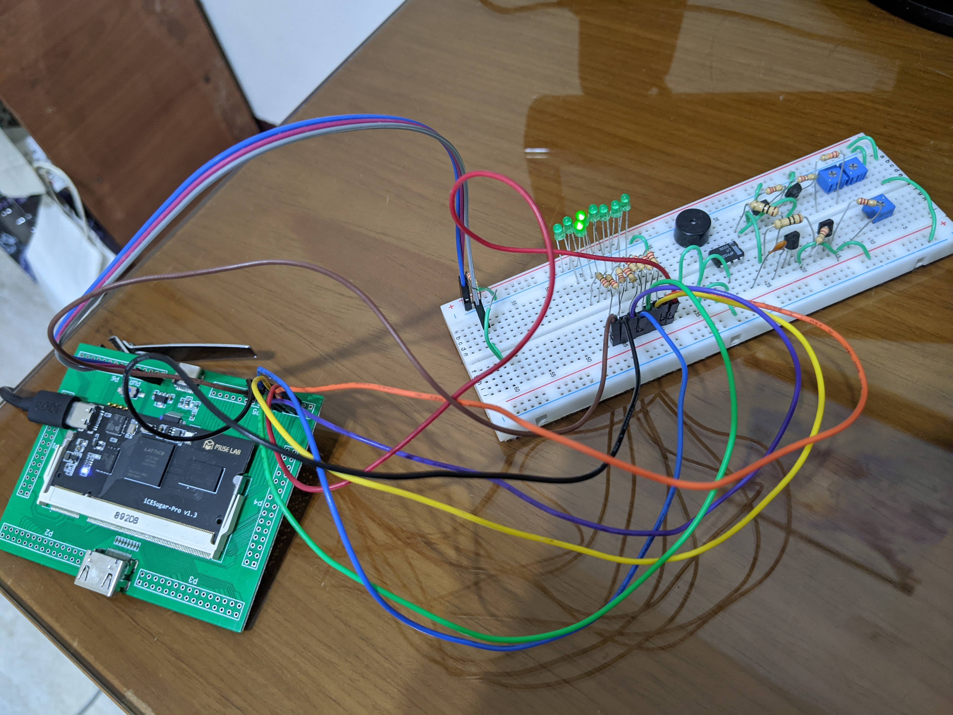
Additionally, a photo debugging rx is attached, where the LED displays the character 0x30 ‘0’ I just pressed.
Conclusion
In this chapter, we upgraded from Verilog to System Verilog. Overall, it was a minor syntax upgrade, without too many structural changes. After spending some time, we successfully implemented UART tx/rx modules using System Verilog, which might be useful in future projects. Coincidentally, I went to buy an HDMI to VGA adapter at Guanghua Market yesterday, and completed the UART module today. It seems the next step is experimenting with HDMI modules.
The completion of this article is due to strong support from my classmates JJL and phoning, especially since I hadn’t touched Verilog for almost a decade. Thanks to the two industry experts supplementing my System Verilog knowledge, this project was smoothly completed.