This content is translated with AI. Please refer to the original Traditional Chinese version (zh-TW) for accuracy.
I’ve finally reached my long-hidden ultimate goal.
That’s right, when I got this FPGA and was thinking about what to do, the answer I reached after a day was this: Nand2Tetris
,
actually building this CPU with FPGA. The previous UART, HDMI, BRAM were just appetizers, in fact, I am playing a very big game.
Of course, since we are using Verilog, we won’t really start building up from NAND gates but instead implement with Verilog’s built-in operations,
so the parts in the first and second chapters of nand2tetris where NAND gates to logic gates and adders are made are skipped, and we start directly from the ALU.
CPU
ALU

The above diagram is the ALU design from Nand2Tetris, with six control signals zx, nx, zy, ny, f, no, respectively indicating:
- zx: Select input 1 or 0 as x
- nx: not x
- zy: Select input 2 or 0 as y
- ny: not y
- f: out = x+y or x&y
- no: not out
The two output flags indicate whether the output is 0 or negative; this is a purely combinational circuit, and the implementation is very simple, the hardest part might be naming the wires:
module hack_alu (
  input i_zx,
  input i_nx,
  input i_zy,
  input i_ny,
  input i_f,
  input i_no,
  input [15:0] inx,
  input [15:0] iny,
  output logic o_zero,
  output logic o_negative,
  output logic [15:0] out
);

logic [15:0] zerox;
logic [15:0] notx;
logic [15:0] zeroy;
logic [15:0] noty;
logic [15:0] fout;

assign zerox = i_zx ? 0 : inx;
assign notx = i_nx ? ~zerox : zerox;
assign zeroy = i_zy ? 0 : iny;
assign noty = i_ny ? ~zeroy : zeroy;
assign fout = i_f ? notx + noty : notx & noty;
assign out = i_no ? ~fout : fout;

assign o_zero = out == 0;
assign o_negative = out[15] == 1;

endmodule
That’s right, that completes the implementation.
Register and PC
The registers and PC are sequential components, storing the input value into a flip-flop when the clk arrives:
module hack_pc (
  input clk,
  input rst,
  input inc,
  input load,
  input [15:0] in,
  output logic [15:0] out
);

always_ff @(posedge clk or negedge rst) begin
  if (!rst) begin
    out <= 0;
  end
  else if (load) begin
    out <= in;
  end
  else if (inc) begin
    out <= out + 1;
  end
end
endmodule
Removing the inc line transforms it from a pc into a register.
module register (
  input clk,
  input [15:0] in,
  input load,
  output logic [15:0] out
);

always_ff @(posedge clk) begin
  if (load) begin
    out <= in;
  end
end

endmodule
CPU
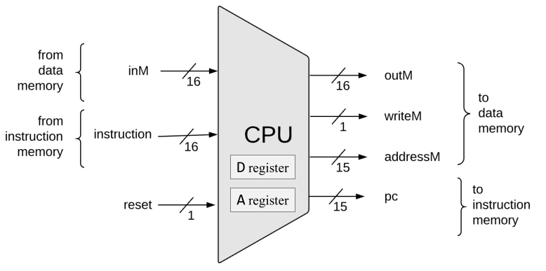
The Nand2Tetris CPU interface is as follows:
- rst: reset CPU
- instruction: instruction from ROM
- inM: content read from specified memory address in RAM
- outM/addressM/writeM: content to write to RAM, address, whether to write
- pc: address for the next instruction fetch from ROM
This interface can be easily translated into a Verilog implementation:
module hack_cpu (
  input clk,
  input rst,
  input [15:0] instruction,
  input [15:0] i_memory,
  output logic o_we,
  output logic [15:0] o_out,
  output logic [15:0] o_addr,
  output logic [15:0] o_pc
);
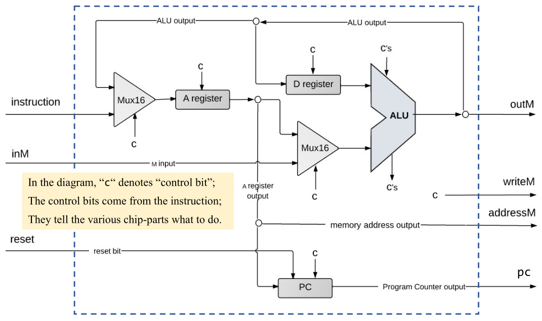 The architecture of the Hack CPU is shown above. It contains two registers, the D (Data) Register and the A (Address) Register;
as the name suggests, the value in the A register indicates the address in Memory currently being accessed, and the D Register is for data used in computations.
The architecture of the Hack CPU is shown above. It contains two registers, the D (Data) Register and the A (Address) Register;
as the name suggests, the value in the A register indicates the address in Memory currently being accessed, and the D Register is for data used in computations.
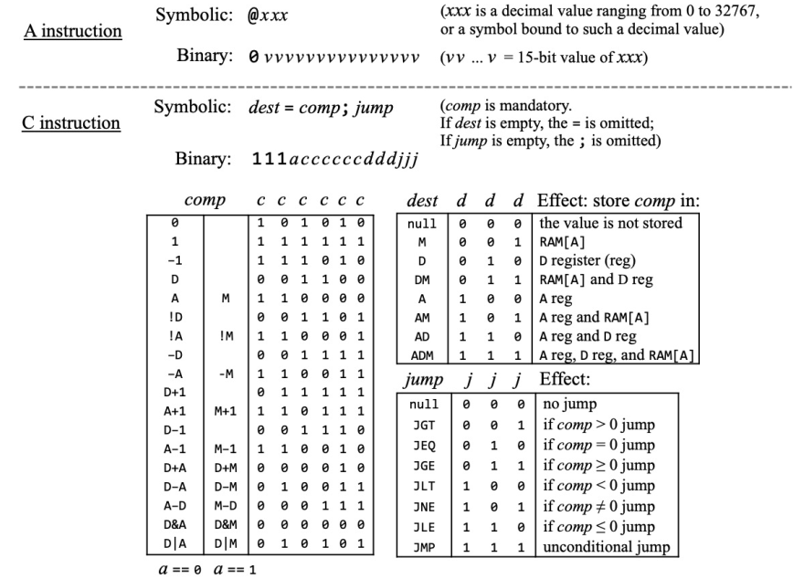
The Hack CPU has only two types of instructions:
- A instruction, starting with 0, indicating to store the value of the following 15 bits into the A register.
- C instruction, starting with 1; the following bits represent:
- a: select input to ALU as A register or memory input.
- c: decide operation to perform in ALU.
- d: Destination, whether to write the computation result into A register/D register/RAM.
- j: Jump, whether to jump according to the computation result.
The implementation internally is as shown in the diagram, and basically, it’s all about wiring things up, as shown in the implementation:
logic [15:0] inx;
logic [15:0] iny;
logic [15:0] addr_instruction;
logic [15:0] a_out;
logic [15:0] alu_out;
logic [15:0] next_pc;
logic f_zero;
logic f_negative;
logic jump;

logic is_A_inst, is_C_inst;
assign is_A_inst = (instruction[15] == 0);
assign is_C_inst = !is_A_inst;

assign addr_instruction = is_A_inst ? instruction : alu_out;
assign iny = instruction[12] ? i_memory : a_out;

always_comb begin
  if (is_C_inst) begin
    case ({instruction[2], instruction[1], instruction[0]})
      3'b000: jump = 0;
      3'b001: jump = !(f_negative || f_zero);
      3'b010: jump = f_zero;
      3'b011: jump = !f_negative;
      3'b100: jump = f_negative;
      3'b101: jump = !f_zero;
      3'b110: jump = f_negative || f_zero;
      3'b111: jump = 1;
    endcase
  end
  else begin
    jump = 0;
  end
end
The section above first declares some wires, and the two ternary operators in assign correspond to the two muxes in the diagram; the jump signal implementation doesn’t need to be like nand2tetris, drawing a Karnaugh map to reduce it into logic gates. In Verilog, we don’t do that; we let the synthesizer handle it.
hack_pc pc (
  .clk(clk), .rst(rst),
  .inc(1'b1), .load(jump),
  .in(a_out + 1), .out(next_pc)
);

register register_d (
  .clk(clk),
  .in(alu_out),
  .load(is_C_inst && instruction[4]),
  .out(inx)
);

register register_a (
  .clk(clk),
  .in(addr_instruction),
  .load(instruction[5] || is_A_inst),
  .out(a_out)
);

hack_alu alu (
  .i_zx(instruction[11]),
  .i_nx(instruction[10]),
  .i_zy(instruction[9]),
  .i_ny(instruction[8]),
  .i_f(instruction[7]),
  .i_no(instruction[6]),
  .inx(inx),
  .iny(iny),
  .o_zero(f_zero),
  .o_negative(f_negative),
  .out(alu_out)
);

assign o_out = alu_out;
assign o_addr = a_out;
assign o_we = !is_A_inst && instruction[3];
assign o_pc = jump ? a_out : next_pc;
This section wire-connects a few components, completing the CPU. In my CPU design, there are some modifications to the inputs and outputs of o_pc and the PC module, related to the ROM portion to be discussed later.
Memory
The memory is probably the biggest hassle this time. In nand2tetris design, each address has 16 bits of data:
- ROM addresses 32 K
- RAM addresses 16 K
- display memory addresses 8 K
- 1 byte of keyboard input, which we’ll ignore for now
As mentioned in the previous block memory part, we have 56 DP16KD, configured with a data width of 16 bits, each DP16KD can store 1K entries, so we only have 56 K entries.
Theoretically, 56 = 32 + 16 + 8, but we encounter a big problem here; according to the DP16KD documentation, it should be a True Dual Port memory unit,
meaning it supports two sets of inputs and outputs, can run on different clock cycles, addresses, and data, but the problem is: yosys doesn’t handle this useless waste.
I implemented dual-port block memory, and when synthesized with yosys, it couldn’t map to DP16KD, which is a long-standing bug in yosys’s memory model a long-standing bug , with others reporting similar issues , although the issue was opened in 2020/04, it’s still unpredictable when it might be fixed, which is common in the open-source world.
So, what happens if Dual Port memory can’t be placed? The answer is that yosys will replace the Dual Port with two Single Port memories and find a weird way to synchronize both sides. The only component needing dual-port is the display memory, which needs to be accessed separately by CPU and HDMI, requiring double or 16K addressing, depleting the block memory.
I used the simplest solution by reducing the ROM size, currently designing as:
- ROM addresses 16K
- RAM addresses 16K
- display memory addresses 8K + 8K A total of 48 K.
ROM
Let’s implement the ROM. The section with `ifdef is for verification with Verilator, as Verilator doesn’t accept writing if (FILE) this way, so they must be separated with ifdef;
in ROM we use readmemb to load nand2tetris code into ROM, similar to how image data was loaded in the previous chapter.
module rom (
  input clk,
  input [DEPTH-1:0] addr,
  output logic [WIDTH-1:0] data
);

parameter WIDTH=16;
parameter DEPTH=14;
parameter SIZE=(1<<DEPTH);
parameter FILE="rom.hack";

logic [WIDTH-1:0] ram [0:SIZE-1];

`ifdef verilator
initial begin
  $readmemb("rom.hack", ram);
end
`else
initial begin
  if (FILE) begin
    $readmemb(FILE, ram);
  end
end
`endif

always_ff @(posedge clk) begin
  data <= ram[addr];
end

endmodule
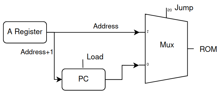
Because ROM also clocks, meaning after the address is ready, the data outputs after one clock, which in the original nand2tetris design results in a bubble.
Rendered in a table, the timing roughly appears as follows:
| Instruction, ROM output | next PC | PC output |
|---|---|---|
| n, jump to k | k | n+1 |
| n+1 | k+1 | k |
| k | k+2 | k+1 |
You see an additional execution of undesired instruction n+1; since the next instruction needs a clock at PC and another at ROM; one solution certainly could be altering the above ROM to a combinational circuit, though uncertain if it could normally synthesize block memory. Thus, I modified the CPU inputs and outputs related to the PC into what is shown in the diagram , where during jumps, the jump address won’t be sent to the PC initially, but through a mux directly to the ROM, instead sending jump address +1 to the PC, so that it continues execution of the next instruction immediately after the jump.
RAM
There’s nothing special about RAM; it declares 16K of RAM and 8K of screen, CPU accesses this memory separately; GPU accesses only the screen.
module ram (
  input clk,

  // CPU rw side
  input we,
  input [DEPTH-1:0] addr,
  output logic [WIDTH-1:0] data_rd,
  input [WIDTH-1:0] data_wr,

  input [DEPTH-1:0] gpu_addr,
  output logic [WIDTH-1:0] gpu_data
);

localparam WIDTH = 16;
localparam DEPTH = 16;
localparam RAM_SIZE = (1<<14);
localparam SCREEN_SIZE = (1<<13);

// 16K cpu ram
logic [WIDTH-1:0] ram [0:RAM_SIZE-1];
// 8K screen ram
logic [WIDTH-1:0] screen [0:SCREEN_SIZE-1];

logic [WIDTH-1:0] ram_data;
logic [WIDTH-1:0] screen_data;

// CPU side
always_comb begin
  ram_data = ram[addr[13:0]];
end

always_ff @(posedge clk) begin
  if (we && addr[15:14] == 2'b00) begin
    ram[addr[13:0]] <= data_wr;
  end
end

always_comb begin
  screen_data = screen[addr[12:0]];
end

always_ff @(posedge clk) begin
  if (we && addr[15:14] == 2'b01) begin
    screen[addr[12:0]] <= data_wr;
  end
end

always_comb begin
  if (addr[15:14] == 2'b00) begin
    data_rd = ram_data;
  end
  else if (addr[15:14] == 2'b01) begin
    data_rd = screen_data;
  end
  else begin
    data_rd = 0;
  end
end

// GPU side
always_ff @(posedge clk) begin
  gpu_data <= screen[gpu_addr[12:0]];
end

endmodule
top module
The foundation of the module is last time’s broadcast of Ni Ge Golden Humor.
logic [15:0] rom_addr;
logic [15:0] instruction;
logic [15:0] mem_out;
logic mem_we;
logic [15:0] cpu_out, addr;
logic [15:0] gpu_addr, gpu_data;

rom #(
  .WIDTH(16),
  .DEPTH(14),
  .SIZE(1<<14),
  .FILE("rom.hack")
) rom_i (
  .clk(clk),
  .addr(rom_addr[13:0]), .data(instruction)
);

hack_cpu cpu (
  .clk(clk), .rst(rst),
  .instruction(instruction), .i_memory(mem_out),
  .o_we(mem_we), .o_out(cpu_out),
  .o_addr(addr), .o_pc(rom_addr)
);

ram ram_i (
  .clk(clk),
  .we(mem_we),
  .addr(addr), .data_rd(mem_out), .data_wr(cpu_out),
  .gpu_addr(gpu_addr), .gpu_data(gpu_data)
);
This part wires up the connections between modules, with gpu_addr and gpu_data coming from the image source previously, originally using counterX/counterY to get corresponding positions, with pixel data as 1 byte size.
Nand2Tetris makes each pixel as one bit, with a 512x256 screen size totaling 131072 pixels, making up RAM with 8K addresses and 16 bits for each content. With counterX/counterY, it calculates which 16-bit data is taken out from an address and displays it as either a white or black pixel; the calculations between address, data, and pixel are as follows:
assign gpu_addr = (counterY << 5) + (counterX >> 4);

always_comb begin
  if (counterX >= 512 || counterY >= 256) begin
    pixel = 24'd0;
  end
  else begin
    pixel = (gpu_data[counterX & 4'hf]) ? 24'hffffff : 0;
  end
end
Debugging
Once the CPU is prepared, the code is written into ROM directly through the rom.hack file, and execution begins at address 0 upon powering up. Initially, I used RectL.asm to test, which is supposed to draw a small rectangle in the top-left corner of the screen, but issues arose. After debugging with Verilator, I discovered two bugs in my homemade assembler:
- The first was not considering leading/trailing spaces, causing jump string judgment errors, resulting in the asm writing jump without actual jumping.
- Another mistake was not handling A+D vs D+A, D+M vs M+D differences, spitting out incorrect commands.
Finding these bugs was so funny I almost died laughing.
Executing
Here’s the testing code I used:
Sys.jack
class Sys {
  /** Performs all the initializations required by the OS. */
  function void init() {
    do Screen.init();
    do Main.main();
    do halt();
  }

  /** Halts execution. */
  function void halt() {
    while (true) {
    }
  }

  function void oneMilliSecond() {
    var int i;
    let i = 0;
    while (i < 275) {
      let i = i + 1;
    }
    return;
  }

  function void wait(int duration) {
    var int i;
    let i = 0;
    while (i < duration) {
      do oneMilliSecond();
      let i = i + 1;
    }
    return;
  }
}
Sys provides the oneMilliSecond function and the wait function, where 275 for oneMilliSecond is experimentally determined. Theoretically, you could look up the assembly to see how many instructions this while loop executes, then calculate how many iterations it takes to execute 25000 instructions, though I was lazy… then my self-written compiler gives me unreadable code…
Screen.jack
class Screen {
  static array SCREEN;
  static int SCRSIZ;
  static boolean COLOR;

  /** Initializes the Screen. */
  function void init() {
    let SCREEN = 16384;
    let SCRSIZ = 8192;
    let COLOR = true;
    return;
  }

  function void fillScreen(bool on) {
    var int i;
    let i = 0;
    while(i < SCRSIZ) {
      let SCREEN[i] = on;
      let i = i + 1;
    }
    return;
  }
}
Screen originally provides more necessary drawing functions but deletes them leaving only fillScreen to turn the whole screen black or white for testing purposes.
Main.jack
class Main {
  function void main() {
    while(true) {
      do Screen.fillScreen(true);
      do Sys.wait(1000);
      do Screen.fillScreen(false);
      do Sys.wait(1000);
    }
    return;
  }
}
Main function repeatedly toggles between black and white. The whole compilation process uses my own tool to compile, including JackCompiler to compile Jack into .vm file; VMTranslator compiles .vm file into assembly; finally, HackAssembler in Rust interprets into Nand2Tetris binary; output binary is the format that can be directly used with readmemb into ROM.
This is a video of execution:
nand2tetris example
There are three example programs inside nand2tetris:
- Screen
- Output
- String
After final testing, only Screen Test can successfully run; the other two tests are 34K and 26K in size, exceeding our ROM capacity limit.
While publishing, the video above shows when I was making the screen black and white, because my hardware design bugged, causing the test image provided by the nand2tetris course to display broken, after a week of debugging, through Verilator outputting the waveform, with help from a strong colleague over the phone, gradually fixed two different bugs.
Phoning: There’s no problem unreadable by waveform. If… there’s no ifs! If not… there’s no ifs!
So why did I post the article before fully fixing the bugs? I just couldn’t hold it thinking it’s a big deal to write a CPU.
Firstly, the first bug was in the ram part where reading screen data was written as clocked. CPU failed to read screen data one cycle late, hence when CPU writes into the screen, the current screen data cannot be read, and it rewrites it. This made no difference when the whole screen turns white or black because every data written was all 1s or 0s; but when using nand2tetris’s Screen API, drawing pixel one by one resulted in drawing one line, with only the last bit written into each 16 bits being shown.
The second issue is also related to cycles, in the ram reading part we wrote:
// CPU side
always_comb begin
  ram_data = ram[addr[13:0]];
end

// The first issue was screen_data here, written as always_ff which made data one cycle late
always_comb begin
  screen_data = screen[addr[12:0]];
end

// GPU side
always_ff @(posedge clk) begin
  gpu_data <= screen[gpu_addr[12:0]];
end
Well okay, thus GPU gets data from ram when it delays by one cycle, why not change this part to always_comb with no delay?
The answer is I changed it, then yosys wouldn’t use block memory for RAM anymore, instead splitting it into 16K memory using another component TRELLIS_SLICE, but that immediately exceeds the limits of icesugar-pro, so we can only allow gpu data to delay by one cycle.
And because gpu data delays one cycle, in the GPU itself needs to correspondingly adjust, determining output using the previous cycle’s index, preventing graphics from breaking:
logic [3:0] index;
assign index = counterX[3:0] - 1;

always_comb begin
  if (counterX >= 512 || counterY >= 256) begin
    o_pixel = 24'd0;
  end
  else begin
    o_pixel = (i_data[index]) ? 24'hffffff : 0;
  end
end
With these two patches, the example in nand2tetris can execute normally; the result is as follows:

The full execution takes about 40 seconds, roughly equating to executing approximately 1G instructions… Due to the extreme simplification of this CPU with few instructions available, and my compiler lacking optimization, writing one pixel might take hundreds of instructions to complete.
Conclusion
After testing with nand2tetris examples, the CPU operation should be fine, apart from the assembler, no issues have been found in other compilers and VM translators. Although it’s a simple CPU, it’s the first time implementing a CPU on an FPGA, giving quite a sense of achievement; Nand2Tetris’ keyboard is not yet implemented, this part has some considerations that should be discussed in the next post.
The current system still has block memory constraints because Nand2Tetris CPU capabilities are very simple, even simple computations require a lot of instructions for execution, leading to Nand2Tetris code being bigger than expected, fully embedding the OS services almost makes all examples exceed our 24K capacity limit, not to mention writing Tetris on it.
There are certainly multiple solutions to this issue:
- Allow yosys to support dual port memory, then display wouldn’t consume two times and need only 8K, but the issue being stuck suggests it’s not short-term feasible.
- Find a way to connect to DRAM, then use all block memory 56K as ROM, but it’s also somewhat challenging.
Xilinx, just pay to win, money solves everything
In short, we’ve conceptually verified the possibility of implementing Nand2Tetris CPU with FPGA under this chapter, the next step is to implement the interface for the keyboard.