上一章
我們看了怎麼從記憶體中讀取資料放給
IP 模組,這篇我們就反過來,從 IP 模組中送資料給記憶體。
很多東西跟讀取是一樣的,會跳過不少 DMA 相關的介紹,比較簡單一些。
測試用的模組
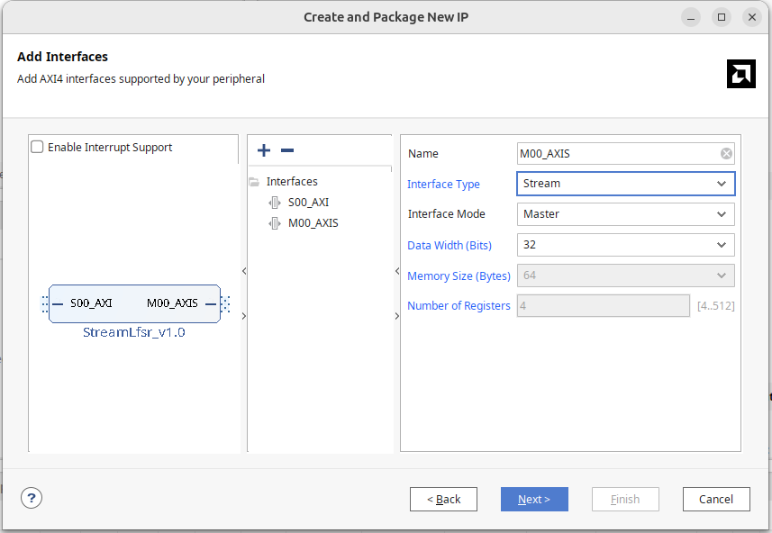
實作一個單向只有 stream 寫入的模組,實作的模組如下:
輸入 32 bits seed、想要輸出的 26 bits 長度(byte) 以及 start 訊號;
啟動用 seed 輸出指定長度的 LSFR 亂數。
因為 LFSR 有很多不同的 taps 形式,看了這篇Table of Linear Feedback Shift Registers 整理選用 32, 30, 26, 25 bits 為 taps。
同樣我們請 AI 幫我們實作:
Help me write a StreamLfsr module, with taps 32, 30, 26, 25
Input is the 32 bits initial seed, 26 bits output byte length, and 1 bit start signal
Output 32bits AXI Stream, which should output designated length of bytes by keep.
下面是 AI 實作,這次倒是做得不差:
module StreamLfsr (
    input  wire        clk,
    input  wire        rst_n,

    // Control Signals
    input  wire [31:0] initial_seed,
    input  wire [25:0] byte_length, // Total bytes to output
    input  wire        start,
    output reg         busy,

    // AXI-Stream Master Interface
    output wire        m_axis_tvalid,
    input  wire        m_axis_tready
    output wire [31:0] m_axis_tdata,
    output wire [3:0]  m_axis_tkeep,
    output wire        m_axis_tlast,
);

    reg [31:0] lfsr_state;
    reg [25:0] bytes_remaining;

    // LFSR Logic: Generate 32 new bits per cycle
    // This loops the single-bit shift 32 times combinationally
    function [31:0] next_state;
        input [31:0] curr;
        integer i;
        reg feedback;
        begin
            next_state = curr;
            for (i = 0; i < 32; i = i + 1) begin
                feedback = next_state[31] ^ next_state[29] ^
                           next_state[25] ^ next_state[24];
                next_state = {next_state[30:0], feedback};
            end
        end
    endfunction

    assign m_axis_tdata  = lfsr_state;
    assign m_axis_tvalid = busy;
    assign m_axis_tlast  = (bytes_remaining <= 4);

    // TKEEP logic based on remaining bytes
    assign m_axis_tkeep  = (bytes_remaining >= 4) ? 4'hF :
                           (bytes_remaining == 3) ? 4'h7 :
                           (bytes_remaining == 2) ? 4'h3 : 4'h1;

    always @(posedge clk or negedge rst_n) begin
        if (!rst_n) begin
            busy <= 1'b0;
            lfsr_state <= 32'h0;
            bytes_remaining <= 26'h0;
        end else begin
            if (start && !busy) begin
                busy <= 1'b1;
                lfsr_state <= initial_seed;
                bytes_remaining <= byte_length;
            end else if (busy && m_axis_tready) begin
                if (m_axis_tlast) begin
                    busy <= 1'b0;
                end else begin
                    lfsr_state <= next_state(lfsr_state);
                    bytes_remaining <= bytes_remaining - 4;
                end
            end
        end
    end

endmodule
建立 IP
一樣先打包我們的 IP:
- Tools -> Create and Package New IP
- 選擇 Create a new AXI4 Peripheral,模組命名為 StreamLfsr
- 在 AXI 的介面上,新增一個 AXI stream interface,介面設定為 Master
跟 ReadDMA 一樣,會看到一個 M00_AXIS 的模組,內部是一個 FIFO 記憶體,它會不斷重複以下的循環:
- 靜待 32 個 cycles (parameter 可以改等多久)
- 把 FIFO 中的內容完整輸出一次
同樣我們的模組本身就能輸出 AXI stream,就把這個 StreamLfsr_v1_0_M00_AXIS 給刪掉。
將 AXI stream 帶的介面:
- m00_axis_tvalid
- m00_axis_tready
- m00_axis_tdata
- m00_axis_tlast
- m00_axis_tstrb
接入我們模組中即可,生成的 master 介面同樣沒有 keep,可複製 tstrb 埠並改為
tkeep,在 Port and Interface 中映射到 AXI stream keep。
或者,一樣可以自建介面,選擇 axis 並選為 master。
Block Diagram
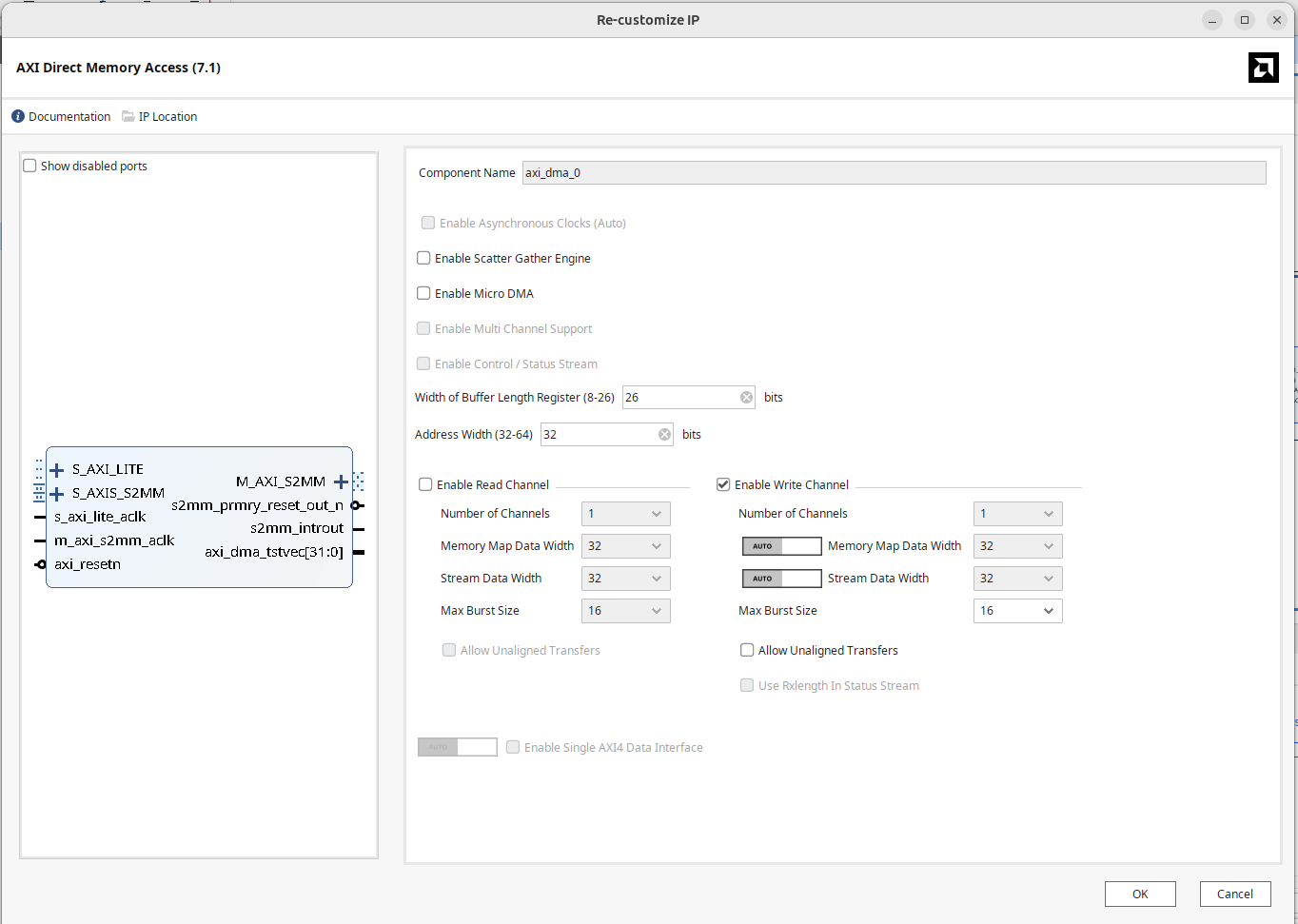
Block Diagram 加入 Direct Memory Access Module。
在 Vivado 裡點兩下開啟 DMA 設定:
- 取消勾選 “Enable Scatter Gather Engine”。
- 設定 Buffer Length Register,依使用量設定 Buffer Length Register 的寬度,設成最大為 26 bits。
- 設定 Address Width 為 32 bits。
- 因為我們這次要把 IP 的資料寫入記憶體,所以只勾選 Write channel。
- Memory-mapped data width 和 stream data width 一樣使用 32 bits
說起來,我也不懂為什麼 DMA 設定,Write 這邊的介面跟 Read 這邊長得不一樣,那個
auto/manual 的 toggle 設計真的是有夠莫名。
要讓 DMA 的 Master 埠存取 DRAM,打開 Zynq PS Block 的 S_AXI HP0,設定 HP 埠的位寬為 64 bits。
完成的 block diagram 如下圖所示:
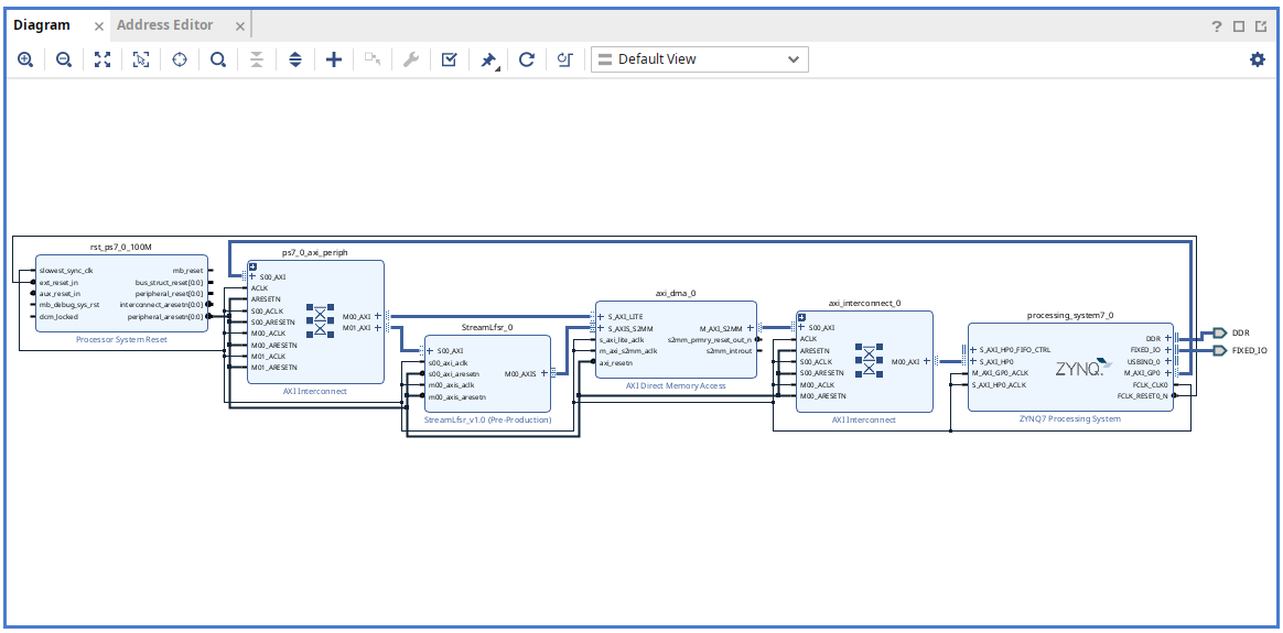
按 F6 進行設計驗證,確保沒有錯誤。
產生 HDL wrapper 與 bitstream。
將產生的 .bit 與 .hwh 放到 PYNQ 板上的資料夾,以便第二部分透過 Python 使用 DMA。
上板測試
為了驗證答案,也請 AI 寫個 python 的 LSFR 進行驗證:
Write me a python LFSR with seed input, tap ad 32, 30, 26, 25
function signature def lfsr(int seed, int byte_length) -> bytes
這是 AI 吐的 python 實作
def lfsr(seed: int, byte_length: int) -> bytes:
    if seed == 0:
        raise ValueError("Seed must be non-zero")

    state = seed & 0xFFFFFFFF
    output = bytearray()

    while len(output) < byte_length:
        # Output current state as little-endian bytes
        output.extend(state.to_bytes(4, byteorder="little"))

        for _ in range(32):
            # Compute feedback bit
            # taps: 32,30,26,25
            feedback = (
                ((state >> 31) ^  # bit 32
                 (state >> 29) ^  # bit 30
                 (state >> 25) ^  # bit 26
                 (state >> 24))   # bit 25
                & 1
            )

            # Shift left and insert feedback bit
            state = ((state << 1) | feedback) & 0xFFFFFFFF

    return bytes(output[:byte_length])
把 .bit 檔載入之後,使用 ? 看看有哪些模組可以呼叫:
from pynq import Overlay, allocate
ol = Overlay("WriteDMA.bit")
ol?

IP Blocks
----------
axi_dma_0            : pynq.lib.dma.DMA
StreamLfsr_0         : pynq.overlay.DefaultIP
processing_system7_0 : pynq.overlay.DefaultIP
看到 axi_dma_0 的 DMA 控制器與 StreamLfsr_0 連接在 AXI Lite 上面的 IP block。
依照我們的設計,可以實作一個 hw_lfsr 的函式,負責分配 IP 模組寫入的記憶體,寫入 seed, byte_length, start 啟動硬體;使用 DMA 的 recvchannel 進行 transfer 將資料填入記憶體。
ip = ol.StreamLfsr_0
dma = ol.axi_dma_0
dma_recv = dma.recvchannel

def hw_lfsr(seed: int, byte_length: int) -> bytes:
    buffer = allocate(shape = (byte_length,), dtype = np.uint8)
    ip.write(0, seed)
    ip.write(4, byte_length)
    ip.write(8, 1)
    dma_recv.transfer(buffer)
    return buffer.tobytes()
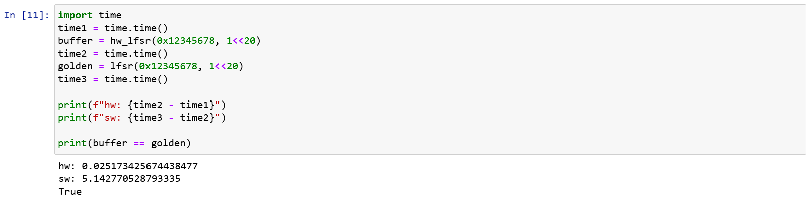
執行結果:
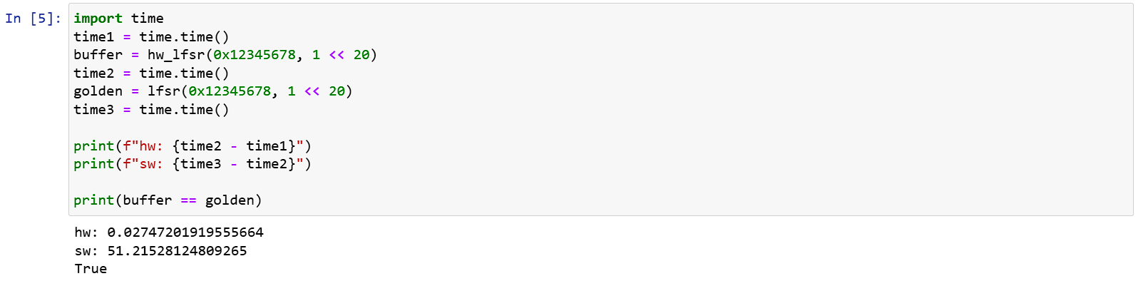
軟體加速
上面可以看到,雖然輸出了 1MB
的資料硬體和軟體輸出了一樣的結果,但軟體實在是太慢了,光是 1MB 就要算 50s 。
顯然是函式每次只生成一個 bit 的問題。
加速為每次生成 16 個 bits,修改如下:
def lfsr(seed, n):
    if seed == 0:
        raise ValueError("Seed must be non-zero")
    state = seed & 0xffffffff
    output = bytearray()
    while len(output) < n:
        output += state.to_bytes(4, 'little')
        for i in range(2):
            feedback = (state >> 16 ^ state >> 14 ^
                        state >> 10 ^ state >> 9) & 0xffff
            state = ((state << 16) | feedback) & 0xffffffff
    return bytes(output[:n])
再次執行的結果,加速不少:
從這裡也可以看出硬體跟軟體(雖然這裡是 python 啦)的速度差,對硬體來說,因為 Lsfr 設計簡單,IP 的頻率可以上到 100MHz,1MB 的亂數所需時間計算為 2.6 ms 就能執行完畢,搭配 AXI Stream 直接寫入記憶體,能輕鬆跑得比軟體還要快。
Last 的問題
在 AXI Stream 中,Last 用來標示整個傳輸的結束,由於硬體端處理 DMA 的模組是依照 AXI stream 規格實作的,因此它也會尊重這個 bit 的結果。
如果我們把模組設定成無視設定,只要輸出 100 筆資料就拉 last
埠,那麼在 driver 的部分也只能拉 100 筆,如果試著讀 150 筆,因為在第
100 筆就看到 last 了,後續的資料 driver 都會無視填入 0。
反過來如果 driver 只拉 50 筆,第 50 筆沒有 last 信號,driver
就會陷入等待,無法發起下一次的 transfer,這時候除了直接 reset 外就救不回來了。
結論
這篇我們展示怎麼在 Xilinx FPGA 上連接 DMA,並寫一個簡單的模組來驗證 DMA 寫入真的有運作,只要組合讀取與結合兩種 AXI Stream,就能創造同時有 DMA 讀取與寫入的模組,例如 FIFO。
關於 AXI 的介紹我想就告一段落了,下一個讓我們來看看 Interrupt 吧。