This content is translated with AI. Please refer to the original Traditional Chinese version (zh-TW) for accuracy.
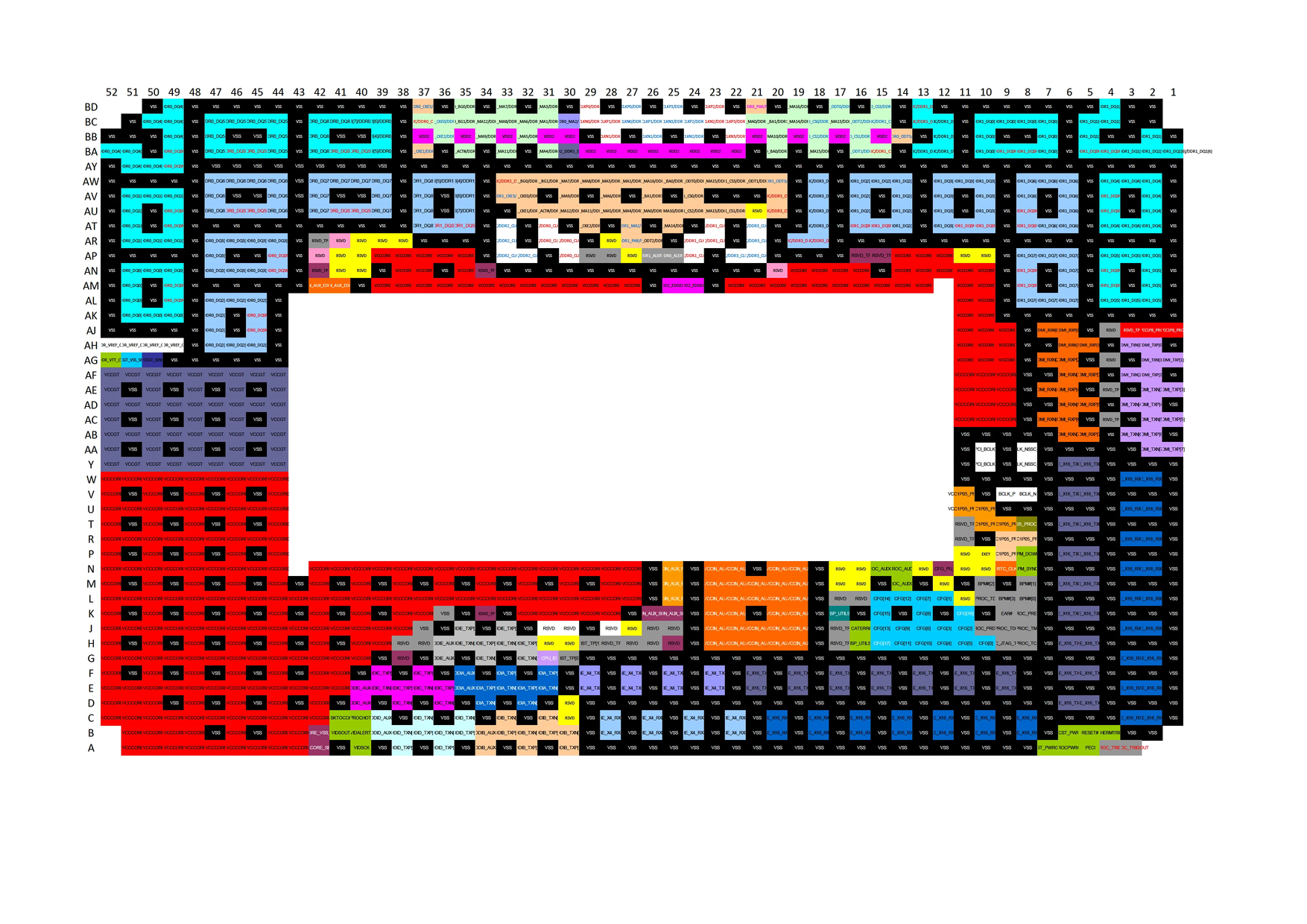
Before talking about APR, let’s first discuss the physical architecture inside a chip, such as pad, bond wire, memory, power ring, power strip, etc., so that everyone can have an understanding of the chip they commonly see, making it easier to write articles with practical software operations later.
This article has been modified extensively after completion, with both the text and images updated significantly to correct any erroneous content. If you are interested in the history of the article, you can search for the history record of the article on Github.
Packaging
The chip we most commonly see in everyday life is probably the black chip with legs, or the CPU chip sitting on a motherboard, where the pins are on the back side as pin connectors or contacts. This is the packaging of the chip.
Depending on the number of pins in the circuit design, different packaging can be chosen. I found the most comprehensive list from Texas Instruments . The packages I am more familiar with include:
- SB: Side-Braze
- CQFJ: Ceramic Quad Flat
- J-leaded CLCC: Ceramic Leadless Chip Carrier
- CQFP: Ceramic Quad Flatpack
Currently, these packages don’t seem to have a unified Chinese translation. You can search for images of each package’s appearance using its name followed by “packages”.
Packaging is the intermediary layer between the chip and the external circuit board. For example, a Side-Braze package can be directly inserted into a breadboard for measurement, while CQFJ, CLCC, CQFP, etc., are more suitable for connecting with self-made circuit boards. Different packages have different sizes and numbers of pins. For example, the SB package might reach a limit at 48 pins, while CQFP can handle several hundred pins. The cost and signal frequency limit of each package vary, and you can select according to your own needs. Personally, I now always choose SB since the number of pins isn’t that high, and there are no frequency requirements.
If we physically destroy the package (open the lid), we will see the underlying die. In reality, the chip is much smaller than imagined, and its large size is due to packaging limitations. Take Intel’s latest 14900K as an example. On the internet, you can find an LGA1700 pinout diagram
for the 14900K. The white area in the middle is where the chip is placed:
 The exterior dimensions of this CPU are approximately 45.0 mm x 37.5 mm, but after removing the lid, the die size is only 257 mm², about 1.6 cm x 1.6 cm, roughly the size of your thumbnail.
Below is a bond wire diagram obtained from a strong peer-classmate. It seems this chip originally wasn’t packaged and was measured on a bare die, so it’s not strictly an opened lid diagram. The middle bare die, after being finished by a wafer foundry, is connected to the surrounding package through bond wire, and the pins on the package allow external power, grounding, and signals to enter the chip:
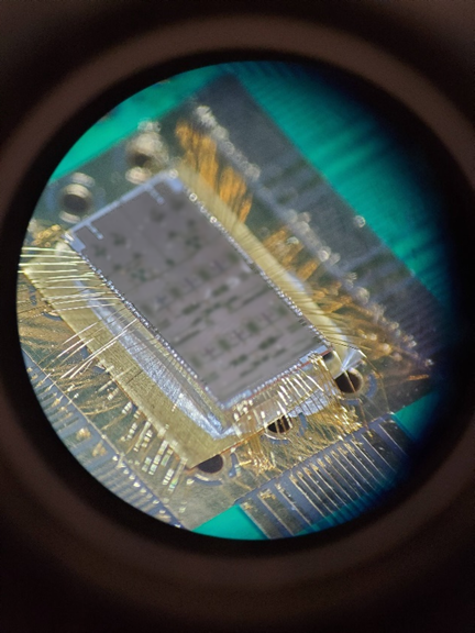
In most processes, the chip utilizes the top-most metal to fabricate a bonding pad around the outer ring of the chip. The bond wire connects this pad to the package. Due to this ring of bond wire acting as a long wire, additional inductance effects are introduced, and in today’s increasingly high-speed chips, these parasitic effects impose additional constraints. Consequently, packaging technologies like Flip Chip have emerged, but that’s straying off topic. I’ll talk about it when I reach this level. If interested, I’ve attached information in the reference material.
Standard Cell Library
Moving into the interior of the chip, from a cross-sectional view, the entire chip from the bottom up is:
- Silicon wafer substrate, refined from sand into a silicon substrate.
- The lowest layer of the transistor chip, including OD oxide diffusion (drain source) and PO Poly oxide (gate) on the wafer.
- Contact, forming the connection point of the transistor, connecting to the upper layer’s metal.
- Metal Connect, metal wires made of copper. Depending on the process, there can be 5, 7, or more than 10 layers of metal used for connections, generally referred to as M1, M2, M3, … M9.
- The top-most Top Metal will have the aforementioned bonding pad. When fabricating the chip, the position of the bonding pad will be opened for bonding wire.
Of course, direct transistor use is mainly in analog, microwave, or MEMS and other special applications. In the digital chip realm, we use the standard cell libraries provided by foundries or IP providers like Arm for design. I found a standard cell library example on a website from Google search, last updated in 2008.
Standard cell libraries provide all sorts of basic logic gates, along with their timing characteristics, electrical properties, etc. Each logic gate has its logic, such as AOI21 representing an And with a NOR gate, a combination that when implemented with CMOS is faster and smaller in area than just using AND, OR gates connected together. To simplify layout efforts, each logic gate is designed according to certain norms, such as:
- Each logic gate has the same height
- The top node connects to the VDD power supply, and the bottom node connects to ground VSS
- Each logic gate uses PMOS and NMOS of the same width
Note that this only applies to general processes. The higher the process level, the more likely special designs of standard cells emerge due to process constraints or performance and power-saving demands.
Above the standard cell library is the part designers handle during layout. Below, we’ll use Minecraft to build a 33x33 chip (this is the closest I’ve found to something that reproduces 3D). Before that, let’s look at definitions for each layer:
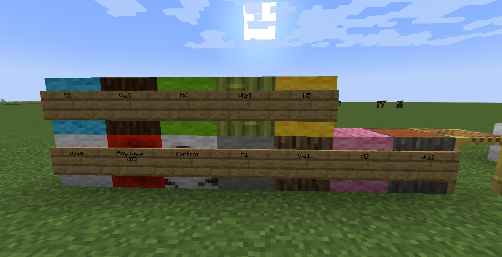 From bottom to top, left to right, it is:
Substrate, each layer of VDD line, Contact, M1, Via1, M2, Via2, M3, Via3, M4, Via4, M5.
From bottom to top, left to right, it is:
Substrate, each layer of VDD line, Contact, M1, Via1, M2, Via2, M3, Via3, M4, Via4, M5.
followpin
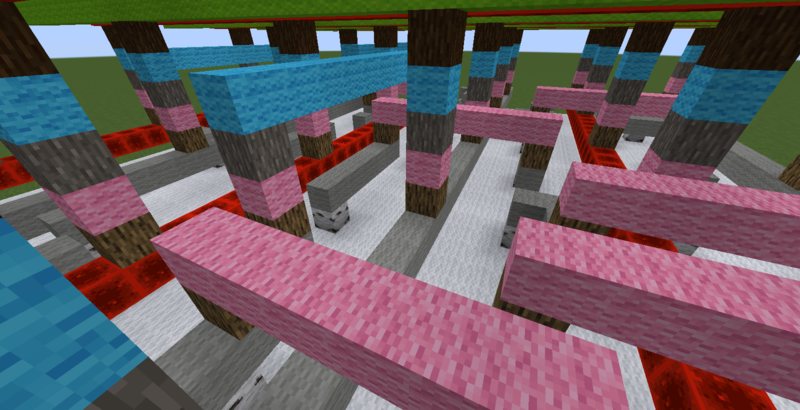
With such formatted logic gates, we will use the bottom-most metal M1 to place horizontal strips called followpins on the chip, one connecting to positive power VDD and one to ground VSS (GND). In layout, logic gates are arranged along the horizontal VDD VSS, like shelves, allowing logic gates to connect to VDD VSS.
The chip connected with followpin looks roughly as the image below shows, with the contact below logic gate nodes connected to the substrate.
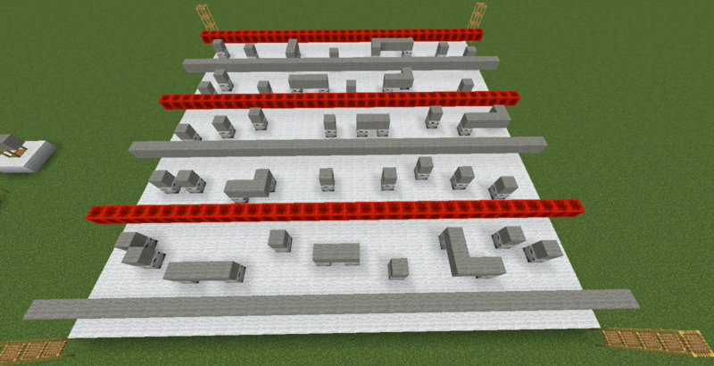
This design can significantly reduce the complexity of a chip. After all, what needs to be connected in a chip includes signal pathways, clock, VDD, VSS, all requiring routing and attention to line width to control voltage drop. Too many variables make it difficult to handle, and using this line method immediately reduces two variables: handling VDD and VSS.
Metal
The Metal layers above, from Metal 2 to Top Metal—let’s cover up to M5 here—each typically have a fixed direction. With followpin already using the bottom-most M1 placed horizontally, the M2-M5 above are sequentially vertical, horizontal, vertical, horizontal. We would directly record M1(H), M2(V), M3(H), M4(V), M5(H).
Metal wires roughly have a few responsibilities:
- Draw Power Ring around the four sides of the chip from the Top Metal down a few layers.
- Add horizontal and vertical mesh Metal Stripe within the chip, connecting the outer Power Ring to the follow pin.
- Metal 2 - Metal 3, and sometimes Metal 4, are used for routing to connect signals to each logic gate’s connection point.
Let’s first look at the Metal stripe part. Generally, M4 is used to start connecting stripe, leaving M2, M3 for routing. Below is a picture with M4 stripe added:
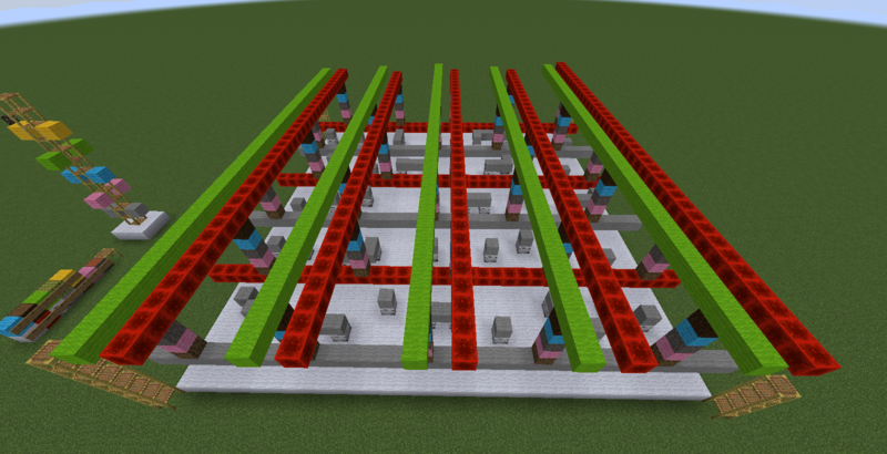
The M4 orthogonal to M1 connects power to the lower M1 via M3, M2. Let’s add another M5 stripe; the upper metal wiring will be wider to conduct more current:
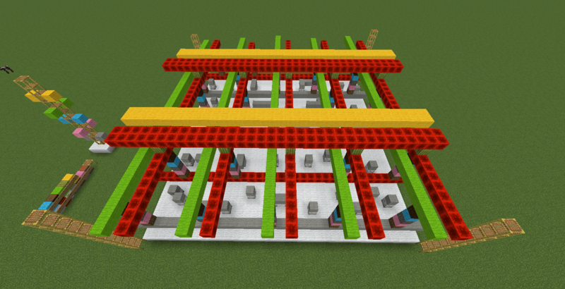
The result of adding a Power Ring shows M4 and M5 in the same direction as the stripe. Together, they line with VDD/VSS:
Here, think about what would happen if the Ring’s direction wasn’t aligned with the stripe?
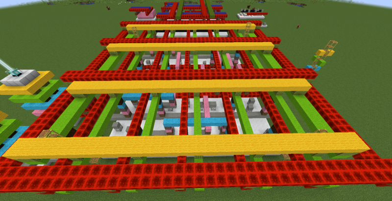
Each Strip layer is connected through Via to the upper layer’s Strip to pass VDD, VSS from the top to the lowest logic gate and also connected to the Ring via Via. A close-up of the Via part shows how the two sets of VDD/VSS are connected—come check out the enlarged view (X3):

As for Route, there’s not much to say—use M2, M3 to connect signal lines from each logic gate below. Since covering this is difficult, let’s just acknowledge it lightly:
Why no stripe for M2 M3 was added, it’s to leave space for route use. However, I once had a version unintentionally connect stripes to M2, M3. Luckily, it ended up okay.
Pad
The structure of a Pad can be imagined as a large metal rod, with the top layer covered in a Top Metal at least 50 um x 50 um in size for bond wire. When making a chip, a circle of pads surrounds the outside to import signals, power, as shown below. First, let’s use Minecraft’s beacon to represent bonding XD:
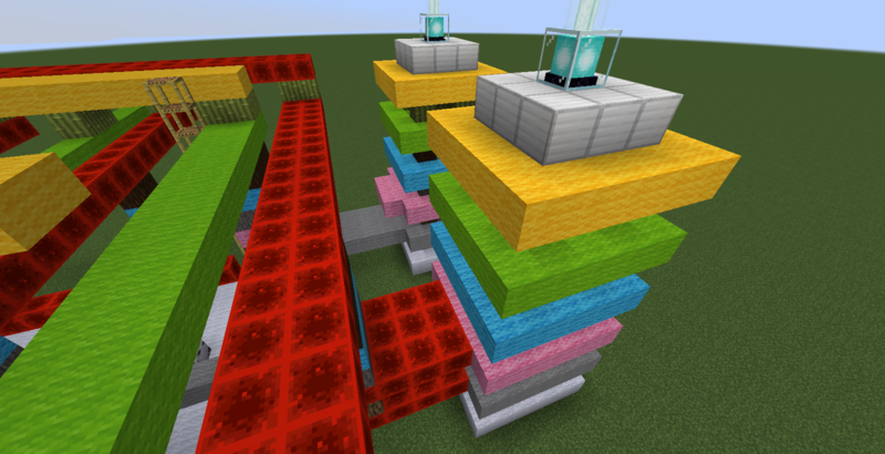
Note that the Pad pulls the signal all the way to the lowest M1 level because an ESD device is hidden below the Pad, requiring connection to the substrate. From M1, M2 left or right is this Pad’s exit pin position (some only use M1), so when adding Power Ring, be careful not to use these layers; otherwise, the Pad lines immediately crash into the Ring, making connection impossible.
Conclusion
Chips are undoubtedly complex things, but we (humans), to make design viable, have already massively simplified the internal structure. For instance, to provide power, we draw Power Strip and Power Ring. To implement complex logic, we use standard cell library logic gates. To connect logic gates, we design chips to add followpin for power supply.
In the next APR practical operation, we’ll see that even these APR software are designed against the above structure. So you might ask, can we design a circuit without connecting followpin or Power Strip and lay out VDD VSS like routing? I would answer yes and no; yes, because physically it’s possible to do so; no, because you have no tool to help do this—APR software generally only routes signal lines and doesn’t handle how to connect VDD/VSS. The structures they can generate are fixed as Power Ring, Power Strip, followpin, etc., and no other structures are available to select.
APR is like AlphaGO—it’s a tool designed for a specific problem, not some generic graph algorithm collection. A friend once asked if it’s possible to use a circuit to write a graph theory problem and let APR tool solve it. It’s like converting all the documents in your computer to static web pages and uploading them online, hoping Google crawls through them then uses Google to search the keywords within your documents. In conclusion, such assumptions are unnecessary. Various chips in the market mostly follow the same structure design and work properly unless you’re an academic institution trying to challenge the basic structure of chip design; otherwise, just follow the method.