This content is translated with AI. Please refer to the original Traditional Chinese version (zh-TW) for accuracy.
After writing Verilog, we move on to a somewhat complex topic, which is discussing what circuit synthesis does. If we use software as a metaphor, what synthesis does is similar to a software compiler. Software is written in a high-level language and then converted into Assembly and machine code through the compiler. In hardware, high-level languages like VHDL/Verilog are used (yes, they are considered high-level languages), and through a synthesis tool, they are converted into gate-level designs. Unless you’re researching standard libraries, not many people write their own adders and multipliers.
Because synthesis tools can directly convert the + and * in Verilog into built-in adders and multipliers. Thus, Synopsys calls it Design Compiler; Cadence simply calls it Genus Synthesis.
To discuss this topic thoroughly, we must first understand the basic structure of circuits. Recently, I came across a great introduction to this topic written by the author of Clash titled Retrocomputing with Clash , where the first chapter provides a detailed explanation.
Basic Structure of Circuits
I assume those who have reached this point understand that digital circuit operations are composed of logic gates. In addition to logic gates, circuits will include elements with storage functions such as latches, flip-flops, and clocks for control.
A clock can basically be thought of as a sine wave that rises and falls at a fixed frequency. With the commonly used positive edge-triggered D Flip Flop, data at its input at the moment the clock transitions from 0 to 1 is captured and presented at the output. The D Flip Flop can only store one bit of information, but by aligning a row of D Flip Flops together, a lot of data can be stored at once, and this is generally referred to as a Register.
Logic gates, flip-flops, and clocks together make up today’s digital circuits.
For example, the course Nand2Tetris that some might have taken is actually more accurately Nand + Register to Tetris. In Week 3: Sequential Logic, it treats the register as a known block, which is understandable. Even though it stacks Nands to create registers , understanding the principles and details within can be quite intricate, so skipping it for a course focused on a bigger picture of computer tech is reasonable.
Setup time / Hold time
When encountering registers, we have to talk about setup time and hold time. At the moment of the Clock’s positive edge, the register updates its internal value, requiring the data at a register’s input to be maintained for a period before and after the positive edge. As shown in the diagram below, we want to store 1 in the register:
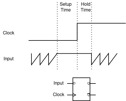
The time prepared beforehand is the Setup Time; the time that needs to be maintained afterward is the Hold Time. Beyond the Setup/Hold Time, it doesn’t matter how the data changes, but around the positive edge, it must be stable, otherwise, the register could capture inconsistent data. Generally, a Setup Time requirement is slightly longer than a Hold time, which can be found in specification sheets. For Texas Instruments’ discrete chip series CDx4HCT74 , the Setup Time is 15 ns, and the Hold Time is 3 ns.
The overall architecture of digital circuits can be illustrated by the following diagram:
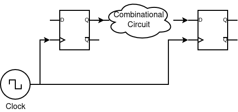
The previous stage register receives data at its output, goes through a series of combinational circuit logic gates, and arrives at the input of the next stage register. Ideally, logic gates don’t consume time, but real circuits do require some computation time. Circuit synthesis ensures that the combinational circuit isn’t too complex, ensuring calculations are completed within one clock cycle while meeting setup and hold time requirements.
For discrete components like CDx4HCT74, a 15 ns delay can be almost neglected, but if a chip operates at a 100 MHz clock, computation time is reduced to just 10 ns. As process technology advances and frequency increases, the setup/hold time of registers also decreases, enabling us to now use GHz-level chips.
SDC Settings
Let’s further expand the basic chip architecture beyond your implemented region, with the solid line blocks representing your implemented region and the outside as what others made or outside the chip:
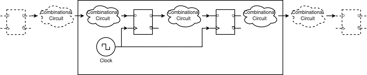
All settings related to synthesis are shown in the diagram above. Since the part beyond the dashed line is invisible to the synthesis tools, how do you calculate the delay from Input to the first Register? The solution is straightforward: the designer needs to set what the Input/Output looks like; otherwise, synthesis cannot be achieved. These settings are referred to as Design Constraints.
Below we introduce some common, nearly mandatory settings for all designs. Others can be looked up if needed. Each setting specifies in which direction to set, challenging the synthesis further.
Common SDC settings can generally be categorized as follows:
Related to Input
set_input_delay
set_input_delay refers to the time consumed from the input register, through external combinational circuits, to the circuit’s input port, in ns. The larger the value, the more time is used externally, making the circuit harder to synthesize. When setting external delays, everyone will typically tell you to set it based on your circuit’s actual situation, but in practice, it’s usually like this: set it to 50% of the clock period, plus an extra 10% for safety, setting it to 60%. For example, with a 100 MHz clock, having a 10 ns period, input/output delay is set to 6 ns.
This way, my circuit uses 40%, and if preceding and succeeding stages also use the same 40% setting, it ensures completion within one cycle.
Input/output delay is divided into two types, one for max delay used in setup time and another for min delay used in hold time. Min delay is usually set to 0. If set to a value like 1, a synthesizer will perceive it as:
- External hold time delay has 1
- Input is directly connected to the register’s port, so this 1 already satisfies hold time (usually only 0.x ns)
- Great, hold time is satisfied, no need to insert a buffer
Hence, don’t randomly set the min delay. Remember this:
If setup time issues arise, just reduce the measurement frequency; if hold time issues arise, it’s hopeless, reducing frequency won’t help.
set_input_transition, set_drive, set_driving_cell
The transition represents how fast a signal on a line changes, in ns. Setting it to 0 is ideal, indicating the signal can instantly rise from 0 to 1; the larger the value, the harder to synthesize.
set_drive/set_driving_cell
This relates to the drive capability of this input stage. A driving circuit’s load model can generally be simplified into a series resistor and a parallel capacitor. Knowing these two values allows calculation of this line’s delay, namely, Wire RC Delay. The name set_drive is somewhat misleading as it sets the R value among the RC mentioned. The smaller the R value, the smaller this path’s delay. If set to 0, the drive ability is unlimited; making it larger adds difficulty to synthesis.
If designing on a cell level with known pre/post states, you can use set_driving_cell, which directly specifies which cell is driving the port. DC can obtain the component model’s transition and drive values from the corresponding library, ensuring the most accurate values.
When implementing a whole chip, the port outside is the actual driving circuit, so you’ll use set_drive and set_input_transition commands to set. Compared to set_driving_cell, using fixed values for set_drive/set_input_transition under different conditions isn’t as precise. I have tried measured chip settings as:
set_drive 0.1 [all_inputs]
set_input_transition 0.5 [all_inputs]
Related to Output
set_output_delay
set_output_delay is analogous to input delay; setting it higher means more time is used from your output port outward, making the circuit harder to synthesize. Applying the same concept, usually, output delay is set to 60% of the cycle time.
set_load
set_load refers to the capacitance magnitude after an output port, with default units in pF. A larger C results in greater delay, making the circuit harder to synthesize.
Like set_driving_cell, if aware of the cell after the circuit, you can use:
set_load [ load_of "<Library>/<Cell>/<port>" ] [ get_port "<port_name>" ]
This configures the load cell, also referencing the library model for the most precise calculation.
If unknown, here’s approximate reference data:
- For synthesizing a cell reaching out to other logic gates, about 0.002 pF; refer to the library settings.
- For synthesizing a top circuit reaching out to chip output pads, approximately 0.05 pF; refer to pad library settings.
- Including output pads together with synthesis reaching out to circuit boards or measuring instruments, roughly 5-10 pF; check manufacturer specs for measuring instruments, such as the input impedance of Arduino’s ATmega328P, found to be 14 pF .
But some instruments don’t have corresponding specs, and I generally learned to set around 20 pF, and for extra assurance, 40 pF can be set; passing the timing check is what’s crucial.
Related to Clock
Clock is probably the most troublesome aspect in all designs, but don’t panic, it’s not so difficult. If you don’t understand the following, relax. It will be discussed again during APR.
create_clock
This is, of course, used to create a clock; set it following instructions, create a clock for each, and set the period to the number of ns required.
create_clock -name clk -period 10 [get_ports clk]
set_ideal_network [get_ports clk]
# set_dont_touch_network [get_ports clk]
set_fix_hold [get_ports clk]
Typically, clock ports are recommended to be set with set_ideal_network, converting this clock path into having zero transition and delay, as clock paths during layout will be handled by APR software generating clock tree synthesis (CTS), so this path’s transition and delay will be decided at that point.
If combinational circuits interrupt your clock, the ideal_network attribute might disappear, and a stronger set_dont_touch_network may be selected to prevent the design compiler from altering your clock network.
set_fix_hold is optional because hold time corrections can be postponed to APR, where wire delay might already satisfy the hold time demands without needing buffer additions. Moreover, as far as I know, APR typically removes all buffers and such on the clock path before executing CTS, so adding this line might slow down Design Compiler’s synthesis time.
Once a clock is available, given that all clock paths will be set as ideal_network, how do we deal with actual imperfections or factors? Consequently, the below three properties need to be added for design compiler analysis.
set_clock_latency
set_clock_latency refers to the time taken from the clock source, through a series of buffers in CTS. During synthesis, absent CTS means actual values are unknown. For a 90 nm process, source latency is generally around 2-3.
set_clock_uncertainty
set_clock_uncertainty corresponds to CTS skew. During APR’s CTS phase, every effort is made to distribute the clock evenly across each register. However, even with perfect leveling, variance persists, affecting data path timing calculations, which needs to be deducted from timing margins. The larger it is set, the harder the chip to synthesize, but setting too small is also risky. If actual skews during CTS aren’t so small, it could cause the chip to fail. Typically, it’s set between 0.1-0.3, depending on the chip’s size, with larger designs set to 0.3 and smaller ones to 0.1. The actual value can be observed after completing synthesis and CTS during APR, and it should be smaller than what was set.
set_clock_transition
This refers to the clock’s time from 10%-90%, and a larger value indicates a slower clock rise, making synthesis harder; I have no experience on this, generally setting around 0.1. Similarly, APR assists in managing this aspect by selecting appropriate buffers during CTS.
Related to DRV
This section’s settings concern the chip’s design rule violation, linked to the library model, distinct from wafer fab design rules. Violating those will halt production immediately, breaching even allows chips to perform suboptimally, like if capacitance is too high causing insufficient signal speed and unmet frequency specifications.
set_max_capacitance
As mentioned, every line has corresponding capacitance, where library tables map capacitance values to the delay and transition of a cell. Synthesis tools use this table to retrieve values for timing calculation. If capacitance value exceeds this table, synthesis tools can only interpolate. Without max capacitance setting, tools will seek the library for the maximum value as default.
set_max_transition
set_max_transition can similarly be checked within the library via the keyword max_transition, setting a value smaller than the maximum. Smaller values mean stricter transition requirements, making synthesis harder.
Moreover, overly strict transition requirements may cause synthesis tools to choose stronger buffers for circuit driving, incurring higher power consumption.
set_max_fanout/set_ideal_network
Finally, max_fanout refers to a component’s output connecting to many loads, significantly burdening that component. Typically, high fanout lines include:
- Clock: Set ideal_network; resolved during CTS in APR.
- reset_n, scan_enable: Set ideal_network, resolved similarly during APR placement.
- Lines holding 0, 1: Ignore; APR will insert TieHi, TieLo cells to resolve.
Special attention is warranted for cases like:
- Clock gating cell output: If synthesis tools can’t identify the clock gating output as part of the clock, ideal_network needs setting.
- Nets with genuinely high fanout: Set max_fanout directly solves this; typically recommended at 20-30. A previously successful design achieved this with 20, allowing synthesis tools to add buffers automatically.
Thus, according to my standard scripts, settings would be configured as follows:
set_max_capacitance 0.1
set_max_transition 0.1
set_max_fanout 25
Quiz
Below are personal experiences occurring due to design circumstances. Listed here to have a laugh test your understanding, utilizing a 100 MHz clock with a 10 ns period.
Case 1
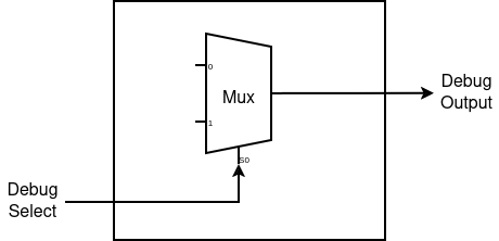
I inserted debug signals in the circuit, selecting the internal signal to view via Input Debug Select, sending the signal to Debug Output, as shown below:
Setting the 60% principle as mentioned above:
set_input_delay 6 [all_inputs]
set_output_delay 6 [all_outputs]
What issue arises with this setting?
Case 2
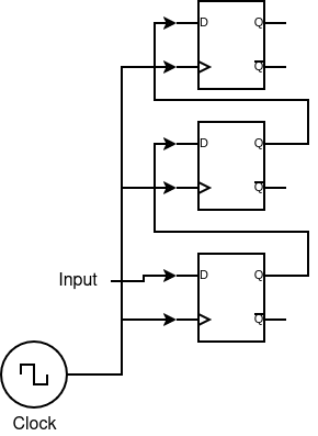
We often have shift circuits in designs, for instance, used in serializer and deserializer as below, demonstrating this deserializer’s RTL behavior:
always @(posedge clk) begin
temp_data <= {temp_data[1:0], in};
end
assign out = temp_data[2:0];
Actual circuit connections are approximately like this:
What timing issue does this circuit present?
Quiz Answers
Case 1 There will definitely be a timing violation. The external input will consume 60%, leaving only 40% time from input to the first register; the same goes for output. However, this circuit lacks registers, meaning the time from input to output is compressed to -20%, ultimately rendering solving impossible.
Case 2 Since there’s only a short connection from register to register, when the clock triggers, as the first register’s output updates, it immediately reaches the second register’s input. The second register’s input doesn’t maintain stability long enough, leading to hold time violation. Synthesis tools typically insert buffers along these lines to rectify this.
Epilogue
Although I initially thought I wouldn’t finish writing this piece, I eventually did. In overcoming challenges with the Design Compiler, I personally consulted substantial information. For instance, asking about set_load often leads to web pages merely describing what it does, lacking a comprehensive macro view of set_load. To address my own questions, writing led to an extensive article which hopefully proves helpful to many, making me so delighted, so happy.
This kind of configuration generally follows similar patterns. Some commands googled direct you to AMD/Xilinx pages—yes, even FPGA synthesis requires these elements. Typically, FPGA tools have preset settings handling this, so check if a project includes a .xdc file, which is a Xilinx Design Constraint file containing related settings. If your FPGA project is complex, such as including low-speed interfaces like UART/IIC, additional xdc configurations are required for Vivado to correctly synthesize the design.
Therefore, familiarizing yourself with these configurations is definitely advantageous.