This content is translated with AI. Please refer to the original Traditional Chinese version (zh-TW) for accuracy.
After discussing design constraint, this article introduces the leading tool for chip synthesis during tape-out - Synopsys Design Compiler.
To be honest, I was a bit hesitant to write this article, because as the leading tool, Design Compiler doesn’t really need my introduction. Cadence also has a corresponding tape-out tool called Genus, but… I only know how to use Design Compiler. If Cadence were to sponsor me for a course, I’d be willing to write an article for them (wink).
The Job of Design Compiler
To put it plainly, synthesis tools convert RTL circuits that we typically write into implementations using various logic gates such as and, or, xor, oai, etc. During this translation process, the synthesis tools also help us focus on PPA:
- Performance: How to synthesize logic gates to achieve the desired frequency
- Power: How to synthesize for the least amount of power consumption
- Area: How to synthesize to minimize the chip area
Among these three constraints, performance takes the highest priority; if the desired frequency isn’t achieved, having a small area and low power consumption is useless. I don’t think anyone would accept buying an i9 but having it perform like a Pentium 4.
Let’s bring out the illustration from the previous section. It’s indispensable to properly set Design Compiler with the understanding of Design Constraint. I suggest everyone review the previous article on Design Constraint multiple times.
After translating to logic gates, the synthesis tool will begin timing checks. Each path between registers is a path, and the synthesis tool will check if the delay of each path adheres to the timing constraints. Below are some actions the synthesis tool might perform:
- If a path is too slow, it will adjust logic gates, optimizing area for performance by using larger, faster circuits to meet timing requirements.
- If a path is too fast, it will insert buffers to add some delay to ensure hold time sufficiency.
- It will address DRV issues like high fanout or excessive capacitance by inserting buffers for proper signal strength.
- It will trade performance for area, selecting slower circuits with smaller areas while still meeting timing requirements.
- For advanced processes, different Vt components are provided . High Vt (HVT) components are slower but consume less leakage power, while Low Vt (LVT) components are faster but leak more power. The synthesis tool will select LVT components on critical paths to meet timing requirements, and use RVT or HVT components on other paths to reduce power consumption.
Setting Up the Design Compiler Environment
The setup file for Design Compiler is .synopsys_dc.setup and is configured in the following order:
- System Setup: Located in $SYNOPSYS/admin/setup’s .synopsys_dc.setup.
- User Setup: Located in the user’s home directory’s .synopsys_dc.setup.
- Project Setup: Located in the working directory’s .synopsys_dc.setup.
Typically, 1 is set by the system administrator and contains settings related to software version during installation; 2 is for personal settings; 3 is unique to each working directory, such as manufacturing process-related settings.
If there are conflicts in settings, personal settings override system settings, and project settings override personal settings. Currently, as I only use one process, I opt for personal settings and not project settings. If your computer luxuriously supports multiple processes, you can switch to project settings.
The contents of .synopsys_dc.setup are as follows:
set search_path "."
set search_path "/path/to/synopsys/db $search_path"
set search_path "/path/to/memory/db $search_path"

set target_library "\
 core_rvt_tt.db \
 core_rvt_ff.db \
 core_rvt_ss.db"

set link_library"\
 * \
 memory_tt.db \
 memory_ff.db \
 memory_ss.db \
 io_tt.db \
 io_ff.db \
 io_ss.db \
 $target_library"

set symbol_library "generic.sdb"
set synthetic_library "dw_foundation.sldb"

set verilogout_no_tri true
set hdlin_enable_presto_for_vhdl "TRUE"
set sh_enable_line_editing true
history keep 2000
Below, I’ll explain the meaning of each of these items in order:
search_path
The paths for locating .v and .db files. One is the db file provided by a foundry for the standard cell process, and the other is to generate db files for the memories used in the chip. Add all these paths to the search_path. To avoid confusion, I habitually separate the db files of standard cells and memories when adding them to the search_path.
target_library
A component library for synthesis logic gates provided by the foundry. The synthesis tool uses components from the target_library to synthesize.
For instance, if you wrote an operator +, and the target_library provides xor and and, the synthesis tool will use xor and and to implement your operator +.
But if the target_library only provides nand, then the synthesis tool will only use nand to build the operator +. A painless achievement for Nand2Tetris.
link_library
A component library for linking; after reading your design, the synthesis tool must find definitions for all components in the link_library. Typically, non-synthesized components are added here, including:
- * denotes searching from design compiler read-in memories
- Contents of target_library
- Tool-generated memory macros
- IO Pads
- Various other macros
There’s a specific explanation about the difference between target_library and link_library , where target_library is used for mapping during synthesis, while link_library is used for referencing after synthesis. Although the probability is quite low, there’s a chance of the synthesis tool composing your circuit using IO Pad cells if it includes IO Pad in the target_library, as part of the design might be too novel. If understanding from software perspective, target_library defines basic assembly instructions used during compilation for high-level language implementations, while link_library defines special assembly instructions. If your circuit directly writes specific avx instructions, the link_library must provide avx instruction definitions. As seen, I’ve included the entire target_library in link_library, because even basic instructions need to be visible by design compiler after synthesis, otherwise it will trigger warnings or errors.
symbol_library
This is needed for the graphical interface to define how components should appear on schematic diagrams. If not provided by the foundry, using the generic.sdb provided by design compiler should suffice, although some components might appear as empty little squares.
synthetic_library
A synthesis library instructing how a high-level function should map to actual logic gates. The dw in dw_foundation refers to synopsys’s DesignWare , which defines how multipliers with pipeline levels 2 through 6 are synthesized and includes many other IP blocks. If a special IP or specific high-level synthesis method is purchased, the .sldb must be filled in here.
Running Design Compiler
Design Compiler can be executed in several ways. One is using the graphical interface:
dv
The Design Compiler graphical interface can do a lot, like viewing how Design Compiler analyzes your design graphically.
Another is text-based, as shown in the next section. Basically, I use a script for everything:
dc_shell
dc_shell -f compile.tcl # Execute compile.tcl
The usage steps of the synthesis tool (that means the contents of the script) roughly divide into the following steps:
- Reading the design
- Setting constraints
- Executing compilation
- Outputting results
Synopsys provides a reference diagram, as shown below:
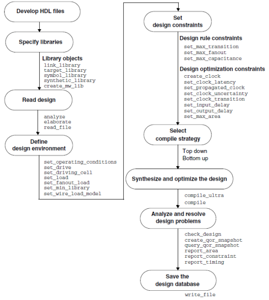
Reading the Design
For the design reading part, the design compiler adopts a VCS-like three-step process:
First, use analyze to read in the design analyze -f sverilog -vcs "-f chip_top.f"
Verilog, SystemVerilog, and VHDL formats can be read; file reading uses the VCS format. Below is the content of chip_top.f:
// top
src/define.sv
src/chip_top.v
src/block_wrap.sv

// add project top directory as include path
+incdir+projdir
-f proj.f
Apart from the top connection, other modules each have a separate .f file. They are included through -f in chip_top.f. In proj.f, similarly, all required .sv files are listed. If your design contains more different blocks, just add .f files.
The second step is elaborate, which analyzes the design,
elaborate $toplevel
Analyzing your design from the $toplevel module and linking the entire design to see what’s inside.
During analyze, the design compiler will convert your design into .pvl and .syn files, which are proprietary binary files that allow design compiler to read designs faster. If messy .pvl, .syn, .mr files in the current working directory annoy you, consider using:
mkdir work
define_design_lib $top_level -path work
To move these intermediate files into the work folder (I rarely used this before writing this article, didn’t know it could be used this way).
The output from elaborate highlights the following:
Inferred memory devices in process
   in routine DMA line 161 in file
    '. ./DMA.sv
==========================================================================
| Register Name  | Type      | Width | Bus | MB | AR | AS | SR | SS | ST |
==========================================================================
| input_data_reg | Flip-flop |  256  |  Y  | N  | Y  | N  | N  | N  | N  |
==========================================================================
This indicates that in this file, a Flip-flop is inferred, and the subsequent columns list corresponding attributes:
- Type: Flip-flop or latch
- Width/Bus: Single bit or multiple bit combination
- MB: Multibit (without specific settings, multibits rarely get deduced, for more details, refer to another article )
- AR/AS: Asynchronous Reset and Asynchronous Set, setting register contents to 0 or 1 via an asynchronous signal.
- SR/SS/ST: Synchronous Reset, Synchronous Set, Synchronous Toggle, setting register contents to 0, 1, or toggle via a synchronous signal.
Here, the key is to first check for errors or failures during elaborate due to syntax errors, and secondly to check if any latches are inferred.
Setting Constraints
Refer to the script in TL;DR below, and review the previous article Design Constraint . After setting the constraints, you can preview using the check_timing to ensure there are no issues with the settings.
Executing Compilation
The compile command in the design compiler starts the synthesis process.
I don’t fully comprehend all the stuff it does behind the scenes, but below I’ll excerpt the major headings in the logs and comment on what I vaguely understand:
Beginning Implementation Selection
Initially, the design compiler substitutes parts of your design with blocks from DesignWare, such as replacing addition with logic gate implementations provided by DesignWare, known as Mapping.
Beginning Mapping Optimization
First optimization, here’s where you first see the table:
| ELAPSED TIME | AREA | WORST NEG SLACK | TOTAL SETUP COST
| DESIGN RULE COST | ENDPOINT | MIN DELAY COST |
- Elapsed time: Current execution time
- Area: Current design area
- Worst Negative Slack (WNS): The biggest margin of error for all Setup time violating paths
- Total Setup Cost: In tools like Xilinx Vivado, this is called Total Negative Slack (TNS), which is the weighted sum of all slack values. By description, it might include slack from max_path (setup) and min_path (hold)
- Design Rule Cost: The margin of difference between current design and user-set goals in design rules
- Endpoint: When the design compiler begins optimization, the current optimization point is listed here. It lists the logic gate (cell) or port being corrected for delay violation. If a design rule is being fixed, the net being fixed is listed.
- Min Delay Cost: This is the TNS of the min_path.
Initially, many design indicators like WNS and area will be large during synthesis, but no worries, they will quickly decrease.
Beginning Delay Optimization Phase
WNS is related to timing constraint. At the end of synthesis, it must decrease to 0, while TNS is the weighted sum of WNS and should also decrease to 0. If WNS can’t be reduced, consider revising the design or relaxing the timing constraints and recompiling.
Beginning Design Rule Fixing
Potential design rules to fix include (min_path) (min_capacitance) (max_transition) (max_capacitance). After correcting the critical delay, buffers will be inserted to fix the design rule, which won’t necessarily be fixed to 0. If set_fix_hold is set, you start to see Min Delay Cost at this stage.
Beginning Area-Recovery Phase
Area optimization begins. Generally, the target for area optimization is 0; the smaller, the better. Let design compiler take care of it and give up when ready. From this order, you can see that for design compiler, the priority is to address timing (delay) issues first, fix design rules second, and finally optimize area. Moreover, regardless of design rule and area optimization causing WNS to deviate from 0, it will be corrected back. If set_fix_hold is configured, buffer insertion begins at this step. In my experience, buffer insertion can be quite slow, so feel free to skip this step if it takes too long and leave the rectification to the layout tool.
Optimization Complete
All tasks have been completed, marking the end of the compile. If further power optimization using HVT is desired, the command
set_leakage_optimization true
compile -inc
can be executed to finish.
Outputting Results
After Design Compiler completes synthesis (typically meaning, run the script and have time for two episodes of anime, then get back), there’s only two things left to confirm:
First is outputting synthesis results, consisting of four types:
- The ddc file of the synthesized design for further optimization in the future, such as swapping to HVT devices or even porting to a new process
- Writing out a standard delay format (.sdf) file. This file records the delay from each node to another location in the circuit, used in post-synthesis simulation
- Writing out the synthesis result: a .v file implementing logic gates. I generally call it .syn.v to indicate it has been synthesized.
- Writing out a constraint file (.sdc), necessary for layout with INNOVUS
Secondly, output the synthesis report generated by Design Compiler. Below in the TL;DR script, various reports are systematically output, with a few being particularly important:
- Check max_timing and min_timing reports to ensure no timing violations
- The area report can provide insight into the area used by each cell, helping pinpoint areas for optimization in your design
- The latch report again confirms the absence of latches in the circuit
- The power report shows the predicted power consumption of the circuit post-synthesis by the design compiler. As design compiler lacks the clock tree information, this power consumption estimate is lower than a layout software or PrimeTime estimation post-layout. My experience varies from 52% to 71% of the final result (and of course, if actual measurements yield even lower power than the estimated by design compiler, that would be another story).
TL;DR
Above is an introduction to how to use design compiler and what it does. However, I know many people who come here might be first-time users of Design Compiler or are rushing to meet deadlines and need to start synthesis quickly. At this time, they don’t want to read everything, just get a workable design compiler script to start running.
I understand all of this. Below I’ve attached the script I use for synthesis. Possibly over 50% is copied from other websites. For those obtainable sources of the following script, I’ll share them here:
- The foundational framework is from Washington University’s class notes Tutorial for Design Compiler .
- STOP_HERE is from CSDN How to Stop DC/PT Execution Script at Any Point .
- The naming rule in the first section of Output may partially come from IThome DC Personal Notes .
At the very least, I can confirm that chips synthesized and created using this script ultimately meet anticipated expectations and have been measured, which might reassure those of you planning to copy directly.
read_file.tcl
The first part is read_file.tcl, and since the elaborate step takes some time, split out a separate read_file.tcl for generating the initial .ddc file for subsequent uses if the design isn’t changed.
########################################
# User Defined Parameters             #
########################################

# Set the top module of your design
set toplevel chip_top

# set the filelist
set filelist chip_top.f

set sh_continue_on_error false
set compile_preserve_subdesign_interfaces true
define_design_lib work -path work

########################################
# Read in Verilog Source Files         #
########################################
analyze -f sverilog -vcs "-f $filelist"
elaborate $toplevel

set filename [format "%s%s" $toplevel "_raw.ddc"]
write -format ddc -hierarchy -output $filename
compile.tcl
The second part is the actual compilation step. There are several aspects that need to be modified:
- Change set_operating_conditions and set_wire_load_model into the actual library you are using.
- Modify the constraint part to your desired numbers, at least change the clock and input/output delay.
- Before running the first compile, uncomment STOP_HERE and check outputs from check_timing and report_net_fanout, firstly ensuring no timing issues, and secondly checking high fanout for inclusion into set_ideal_network.
- set_fix_hold is for specifying hold issue fixes, can be included or not included. Including it might result in design compiler spending a lot of time inserting buffers to fix hold time issues, but these buffers will be completely removed during layout.
- Generally, I’ll set effort to medium first, run a round of synthesis to ensure no problems, then use high to challenge the limits. Of course, the capabilities also differ; for instance, a synthesis of 400 MHz could only converge WNS to 0.1 using medium, while high could reduce it to 0.
- I haven’t tried set_timing_derate. Its objective is to insert a 10% delay during synthesis, enhancing resilience to process variations. But I remember setting it might result in some synthesis issues.
########################################
# User Defined Parameters             #
########################################

# Set the top module of your design
set toplevel chip_top

# set the filelist
set filelist chip_top.f

set sh_continue_on_error false
set compile_preserve_subdesign_interfaces true

# compile design (medium or high)
set effort high

########################################
# Read in Verilog Source Files         #
########################################
# analyze -f sverilog -vcs "-f $filelist"
# elaborate $toplevel
set filename [format "%s%s" $toplevel "_raw.ddc"]
# write -format ddc -hierarchy -output $filename
read_ddc $filename

current_design $toplevel

########################################
# Define constraints                   #
########################################

set_operating_conditions -min <ff.lib> -max <ss.lib>
set_wire_load_model -name Tiny -library <ss.lib>

# 100 MHz main clock
create_clock -period 10 -waveform {0 5} -name clk [get_ports clk]

set_fix_hold              [get_clocks clk]
set_dont_touch_network    [get_clocks clk]
set_ideal_network         [get_ports clk]

# reset and clock gating
set_ideal_network         [get_ports rstn]

set_clock_uncertainty 0.2 [get_clocks clk]
set_clock_latency 1       [get_clocks clk]

set_input_transition 0.5  [all_inputs]
set_clock_transition 0.1  [all_clocks]
set_drive 0.1 [all_inputs]
set_load 20 [all_outputs]

# 6 = 10 * 0.6
set_input_delay -clock clk -max 6 [remove_from_collection [all_inputs] [get_ports "clk"]]
set_input_delay -clock clk -min 0 [remove_from_collection [all_inputs] [get_ports "clk"]]
set_output_delay 4 -clock clk [get_ports "dbg_data"]

# set_timing_derate -late 1.10 -cell_delay [get_cells -hier *]

check_timing
report_net_fanout -high_fanout

# STOP_HERE

########################################
# Design Compiler settings            #
########################################

# max_area
set_max_area 0
set_fix_multiple_port_nets -all -buffer_constants [get_designs *]

compile -exact_map -map_effort $effort -area_effort $effort -power_effort $effort

# power optimization
# set_leakage_optimization true
# compile -inc

########################################
# Output files                         #
########################################

set bus_inference_style {%s[%d]}
set bus_naming_style    {%s[%d]}
set hdlout_internal_busses true
change_names -hierarchy -rule verilog
define_name_rules name_rule -allowed "A-Za-z0-9_" -max_length 255 -type cell
define_name_rules name_rule -allowed "A-Za-z0-9_[]" -max_length 255 -type net
define_name_rules name_rule -map {{"\*cell\*" "cell"}}
define_name_rules name_rule -case_insensitive
change_names -hierarchy -rules name_rule

# save design
set filename [format "%s%s" $toplevel "_opt.ddc"]
write -format ddc -hierarchy -output $filename

# save delay and parasitic data
set filename [format "%s%s" $toplevel ".sdf"]
write_sdf -version 2.1 -load_delay net $filename

# save synthesized verilog netlist
set filename [format "%s%s" $toplevel ".syn.v"]
write -format verilog -hierarchy -output $filename

# this file is necessary for P&R with Encounter
set filename [format "%s%s" $toplevel ".sdc"]
write_sdc $filename

redirect [format "%s%s" $toplevel _design.repC] { report_design }
redirect [format "%s%s" $toplevel _area.repC] { report_area }
redirect -append [format "%s%s" $toplevel _area.repC] { report_area  -hierarchy }
redirect [format "%s%s" $toplevel _reference.repC] { report_reference }
redirect [format "%s%s" $toplevel _latches.repC] { report_register -level_sensitive }
redirect [format "%s%s" $toplevel _flops.repC] { report_register -edge }
redirect [format "%s%s" $toplevel _violators.repC] { report_constraint -all_violators }
redirect [format "%s%s" $toplevel _power.repC] { report_power }
redirect [format "%s%s" $toplevel _max_timing.repC] { report_timing -delay max -nworst 3 -max_paths 20 -greater_path 0 -path full -nosplit }
redirect [format "%s%s" $toplevel _min_timing.repC] { report_timing -delay min -nworst 3 -max_paths 20 -greater_path 0 -path full -nosplit }
redirect [format "%s%s" $toplevel _out_min_timing.repC] { report_timing -to [all_outputs] -delay min -nworst 3 -max_paths 1000 -greater_path 0 -path full -nosplit}

# STOP_HERE
Conclusion
Above covers what I currently know about using Design Compiler and some internal information, and provides the script I currently use for synthesis. I hope this helps you, the readers. Additionally, I’d like to mention that I haven’t encountered Cadence’s Genus synthesis solution, so I can’t write an introductory article on it. However, according to some unreliable sources, Genus seems to already perform better than Design Compiler. Synopsys, please step up your gamestop acquiring and start improving.