This content is translated with AI. Please refer to the original Traditional Chinese version (zh-TW) for accuracy.
In the previous article, we looked at the use of Design Compiler to synthesize our circuits into logic gates. The next steps are to either send it for LEC or do a post-synthesis simulation, after which we will proceed to the main task of using APR to draw the Layout. Before APR, let’s take a single article to see what needs to be prepared before APR.
Be aware that the instructions here are for Cadence’s INNOVUS, and some content is likely different from Synopsys ICC2. If you are an ICC2 user, please be cautious when referencing.
Your Design
Typically, I will name it chip_top.syn.v, which is the verilog file output from the design compiler. It should generally be usable without much processing, with attention to the following points:
- If your design requires pads, it is recommended to include IO cells before sending for synthesis, as mentioned in the Design Constraint article . This way, the synthesis timing will be correct. When the .syn.v output is imported into layout software, these IO pads will connect with the cells set in the .io file below.
- In previous classes, instructors have pointed out that assign syntax should not be present in .syn.v files. One way is to add the following in the design compiler tcl:
set_fix_multiple_port_nets -all -buffer_constants [get_designs *]
This removes the assign syntax. Another is that I have previously thrown verilog files with assign syntax into INNOVUS without issues (and the chip was even measured), so I believe this is no longer a problem.
design constraint .sdc file
In the previous design compiler tcl setting, the write_sdc produced a file. Before importing it into layout software, remove the following settings:
- set_wire_load_model
- set_dont_touch_network
- set_fix_hold
- set_ideal_network
The wire load model is because APR software can know the real wire width and choose the corresponding load model. dont_touch_network, fix_hold, ideal_network are used on clk, reset signals, and since Design Compiler has no physical routing, it will not know the clock tree distribution. These settings prevent it from touching these signal lines, avoiding wasting time handling these high-load lines, but APR software must process these lines. If instructed not to touch them in .sdc, APR will report failure to meet constraints during the clock tree run, halting progress.
IO setting chip_top.io
Although we do cutting-edge work, some things are still most effective with old-fashioned tools. For each tape-out, I prepare an A4 sheet as follows. The top box represents my chip, and use pencil to arrange each pin around it, allowing for easy modification.
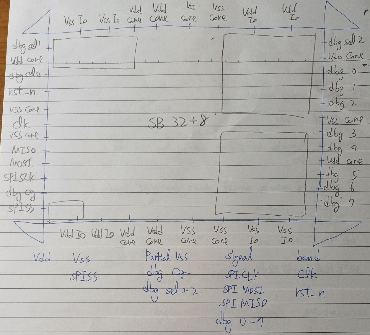
Outside of the pin diagram, open the APR software. After seeing the actual circuit dimensions, you can draw macro information in the grid. For example, in my design, I used four memories, two large and two small ones, and drew their rough positions (also in pencil). Size representation and especially the relative position to each pin should be accurate because power pads will extend metal to the surrounding Power Ring . Hard macro surroundings also need a Macro Ring for power, and the two will clash. Recording this on paper can help avoid issues during pad arrangement, saving numerous problems in the later layout process.
Below the pin diagram, additional information is noted, elaborated on when formally discussing Layout later.
When arranging IO, besides the various signal lines, arrange the power sources used by the Core and IO pins. When first encountering this, planning can be confusing. Generally, you can refer to the guidelines below:
Core Power
To operate the chip, it needs power. Generally, the higher the frequency, the more power it consumes. If not enough power is supplied, the frequency cannot reach its potential. But how do we know how much power the chip will consume?
At each design stage, there are tools providing power estimations:
- After Design Compiler synthesis, use report_power for a power estimate.
- During APR, INNOVUS’ built-in power tool gives another power estimate.
- In the industry, the power estimation standard is Synopsys’s PrimeTime. With simulation of actual behavior, colleagues at major companies say it can be very accurate, though I haven’t personally tried it.
Note that these power estimates are not real power levels, such as Design Compiler lacking clock tree and actual operation behavior information, making them references only. Here’s a comparison of Design Compiler, INNOVUS, and actual measurements from my own tape-outs for reference:
| Design Compiler (mW) | INNOVUS (mW) | Measurement (mW) |
|---|---|---|
| 114 | 220 | 77 |
| 18 | 32 | 10 |
| 58 | 81 | 31 |
You can see that both Design Compiler and INNOVUS tend to overestimate, with INNOVUS overestimating by 2-3 times. However, power should not be understated. Adding a couple more pads is better than not being able to meet the specnot graduating and having to reduce clock speed. Since pads need arrangement before APR, I generally use the Design Compiler’s estimated power with a 1.5-2 times margin, believing it can accommodate INNOVUS’s higher estimates. Then, in the Pad documentation, find how much current or power the VDD/VSS Pads can handle and calculate the required number of VDD/VSS pairs.
IO Power
Next is IO power. The consumption here comes from signal pads requiring power during operation. If VDD/VSS is insufficient, it causes VDD/VSS to fluctuate (e.g., from 1V to 0.99V). If many signals on the chip toggle at once without adequate IO VDD/VSS, it can create substantial issues like in Queen’s “We Will Rock You” . Fluctuations could affect clock stability or trigger a low reset signal, resetting the chip. The IC design industry uses a DF value to describe this. If your chip doesn’t use a Serial Interface and instead lays out many signals, putting it up on a V93000 automatic tester requires calculating the DF value and estimating the needed number of VDD/VSS sets.
Prior to me learning this, refer to Hao Yu’s notes . If a Serial Interface is used, large signals toggling simultaneously is less likely, and 1-2 sets of IO VDD/VSS should suffice.
The workplace’s senior recommendations:
One-third of pins are signal lines; one-third are Core power; one-third are IO power.
I find this estimates power generously, ensuring power is sufficient and signal integrity is assured.
Other Suggestions
Finally, some rules suggested for signal integrity, briefly outlined:
- Use VSS to shield clock pads on both sides, preventing other signals from interfering with the clock.
- Depending on the package, place the Clock on the edge with the shortest path to minimize clock jitter and interference.
- Evenly distribute Core VDD/VSS locations, avoiding concentration on one side, ensuring distant areas don’t starve for power.
- Similarly for the IO Ring, insert IO VDD/VSS within heavy output areas to mitigate measurement affecting fluctuations.
If you look closely, you can see that the diagram above was drawn randomly
IO Setting
After arranging connections, modify the io file as shown. The settings direction follows the coordinate axis. The top and bottom rows follow the X-axis from left to right; the left and right rows follow the Y-axis from bottom to top:
(globals
  version = 3
  io_order = default
)
(iopad
  (top
    (inst name="IVSS_T0"      cell="VSS_io"   place_status=placed)
    (inst name="IVSS_T1"      cell="VSS_io"   place_status=placed)
    (inst name="CVDD_T2"      cell="VDD_core" place_status=placed)
    (inst name="CVDD_T3"      cell="VDD_core" place_status=placed)
    (inst name="CVSS_T4"      cell="VSS_core" place_status=placed)
    (inst name="CVSS_T5"      cell="VSS_core" place_status=placed)
    (inst name="IVDD_T6"      cell="VDD_io"   place_status=placed)
    (inst name="IVDD_T7"      cell="VDD_io"   place_status=placed)
  )
  (left
    (inst name="ipad_ss"                      place_status=placed)
    (inst name="ipad_dbg_clk_gate"            place_status=placed)
    (inst name="ipad_sck"                     place_status=placed)
    (inst name="ipad_mosi"                    place_status=placed)
    (inst name="opad_miso"                    place_status=placed)
    (inst name="CVSS_L0"      cell="VSS_core" place_status=placed)
    (inst name="ipad_clk"                     place_status=placed)
    (inst name="CVSS_L1"      cell="VSS_core" place_status=placed)
    (inst name="ipad_rstn"                    place_status=placed)
    (inst name="ipad_dbg_sel0"                place_status=placed)
    (inst name="CVDD_L2"      cell="VDD_core" place_status=placed)
    (inst name="ipad_dbg_sel1"                place_status=placed)
  )
  (bottom
    (inst name="IVDD_B0"      cell="VDD_io"   place_status=placed)
    (inst name="IVDD_B1"      cell="VDD_io"   place_status=placed)
    (inst name="CVDD_B2"      cell="VDD_core" place_status=placed)
    (inst name="CVDD_B3"      cell="VDD_core" place_status=placed)
    (inst name="CVSS_B4"      cell="VSS_core" place_status=placed)
    (inst name="CVSS_B5"      cell="VSS_core" place_status=placed)
    (inst name="IVSS_B6"      cell="VSS_io"   place_status=placed)
    (inst name="IVSS_B7"      cell="VSS_io"   place_status=placed)
  )
  (right
    (inst name="opad_dbg_data7"               place_status=placed)
    (inst name="opad_dbg_data6"               place_status=placed)
    (inst name="opad_dbg_data5"               place_status=placed)
    (inst name="CVDD_R0"      cell="VDD_core" place_status=placed)
    (inst name="opad_dbg_data4"               place_status=placed)
    (inst name="opad_dbg_data3"               place_status=placed)
    (inst name="CVSS_R1"      cell="VSS_core" place_status=placed)
    (inst name="opad_dbg_data2"               place_status=placed)
    (inst name="opad_dbg_data1"               place_status=placed)
    (inst name="opad_dbg_data0"               place_status=placed)
    (inst name="CVDD_R2"      cell="VDD_core" place_status=placed)
    (inst name="ipad_dbg_sel2"                place_status=placed)
  )
  (topleft
    (inst name="CORNER_TL"    cell="CORNER"   place_status=placed)
  )
  (topright
    (inst name="CORNER_TR"    cell="CORNER"   place_status=placed)
  )
  (bottomleft
    (inst name="CORNER_BL"    cell="CORNER"   place_status=placed)
  )
  (bottomright
    (inst name="CORNER_BR"    cell="CORNER"   place_status=placed)
  )
)
I have summarized the naming conventions for power as follows:
- The first letters I, C represent IO and Core.
- VDD/VSS represents power and ground, though VDD/GND is also an option.
- Suffixes T, B, L, R denote top, bottom, left, right rows, with serial numbers added. Using global serial numbers like VDD1, VDD2… is not recommended, as it requires tracking which numbers appear in each direction, which can be cumbersome.
Aside from power, signals don’t require setting an Input/Output cell. INNOVUS can automatically infer the pad component from the .v file’s cell.
PDK
Prepare PDK files provided by the foundry related to your specific process. Triple-check to make sure you are applying your process settings and not just copying. At minimum, there should be tech.lef, core.lef, and io.lef files, with core divided into slow/fast process variants, all of which are needed. Prior to layout, convert the process model to the OASIS library used by INNOVUS using the import script below:
lef2oa -lef tech.lef -lib macroLib -techRef N90 -useFoundryInnovus
lef2oa -lef core_fast.lef -lib macroLib
lef2oa -lef core_slow.lef -lib macroLib
lef2oa -lef io.lef -lib macroLib
The files provided by the foundry will be in LEF format, containing abstract physical information for the standard cell library, with examples seen on Team VLSI . Tech.lef defines technological LEF files of fundamental parameters, such as:
- Measurement units
- Number of metal layers and vias
- Name, type of each metal
- Whether metal is horizontal or vertical
- Minimum/maximum width
- Recommended spacing between metals
Such comprehensive information allows APR software to follow basic rules during layout.
core_fast/slow.lef are Cell LEFs, containing all available components with information such as:
- Name
- Component type
- Coordinates, dimensions
- Pin name, input/output, nature (signal, power, clock…), pin shape, metal layer usage
Using the analogy of Chip Design Understandable by Grandmothers , LEF provides high-level building descriptions, like a building made of reinforced concrete, with four floors, and getting a catalog from IKEA with options for table sizes, tub sizes, screw placements… APR software utilizes this information to complete the Layout.
Hard Macro
Similar to PDK, Hard Macro (in digital circuits, this usually means memory) also needs to be imported using .lef and .v files before layout. The memories I use are generated from a generator and include:
- hardmacro.lef
- hardmacro.v
- hardmacro.gds
For conversion, use the script containing lef2oa and verilogAnnotate. The former supplies layout, and the latter references the verilog.
lef2oa -lef hardmacro.lef -lib macroLib
verilogAnnotate -refLibs macroLib -verilog hardmacro.head.v
Generally, the verilog output from a memory compiler contains behavioral models. VerilogAnnotate only needs ports and their widths. Trim any behavioral code from hardmacro.head.v as follows:
module hardmacro (clk, cen, wen, addr, i_data, o_data)
input clk;
input cen;
input wen;
input [15:0] addr;
input [31:0] i_data;
output [31:0] o_data;
endmodule
mmmc files
MMMC stands for multi-mode multi-corner, though it’s also referred to as MCMM. The need for MMMC arises with process advancements and increasing chip complexity, introducing more modes for consideration. For instance, originally passing timing might suffice for a chip, but with process shrinking, signal coupling between wires must be addressed, and at small scales, heat dissipation becomes an issue, making power density a concern. Moreover, with added scan chain for testing, additional scan timing analysis is required.
The issue is that timing, power, and coupling were managed by different tools initially. If timing is optimized first, it might end up over-optimized, causing power issues. Addressing cross-mode issues becomes a repetitive and resource-heavy ECO process. In advanced designs, modes and corner cases needing analysis multiply, potentially reaching hundreds of combinations. How to manage this?
Thus, MMMC arises. MMMC combines various modes according to the hierarchical diagram below. Each combination produces a corner condition for software analysis. APR software analyzes conditions to ensure compliance, saving the effort of manually iterating various tests.
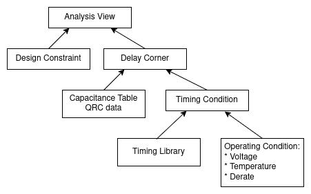
A typical MMMC setting appears as below, again adapted for your process files, copied with caution:
create_rc_corner -name RC_worst
-cap_table {rcworst.captble}
-qrc_tech {rcworst.tch}
create_rc_corner -name RC_best
-cap_table {rcbest.captble}
-qrc_tech {rcbest.tch}

create_library_set -name lib_max -timing
{ slow.lib io_slow.lib hardmacro_slow.lib }

create_library_set -name lib_min -timing
{ fast.lib io_fast.lib hardmacro_fast.lib }

create_opcond -name 0p9v_125c -process 1 -voltage 0.9 -temperature 125
create_opcond -name 1p1v_m40c -process 1 -voltage 1.1 -temperature -40

create_timing_condition -name TC_max -library_set {lib_max} -opcond 0p9v_125c
create_timing_condition -name TC_min -library_set {lib_min} -opcond 1p1v_m40c

create_delay_corner -name DC_max -timing_condition {TC_max} -rc_corner {RC_worst}
create_delay_corner -name DC_min -timing_condition {TC_min} -rc_corner {RC_best}

create_constraint_mode -name CM_func -sdc_files { func.sdc }
create_constraint_mode -name CM_scan -sdc_files { scan.sdc }

create_analysis_view -name AV_func_max
-constraint_mode {CM_func} -delay_corner {DC_max}
create_analysis_view -name AV_func_min
-constraint_mode {CM_func} -delay_corner {DC_min}
create_analysis_view -name AV_scan_max
-constraint_mode {CM_scan} -delay_corner {DC_max}
create_analysis_view -name AV_scan_min
-constraint_mode {CM_scan} -delay_corner {DC_min}

set_analysis_view
-setup {AV_func_max AV_scan_max}
-hold {AV_func_max AV_func_min AV_scan_min}
As seen, it’s merely a text-based translation of the hierarchical diagram above.
- create_rc_corner: Uses capTable PDK RC models and qrctechfiles for RC extraction software, creating an RC scenario.
- create_library_set: Packages all relevant libraries, ensuring to include used hardmacros for analysis.
- create_opcond: Sets operating temperature, voltage, with common ranges of -40
125℃, and voltage of -10%+10%. High-tier processes may add other temperature conditions, such as transistors running faster at high temperatures, necessitating an additional operation condition. - create_timing_condition: Combines operating condition and library.
- create_delay_corner: Combines timing condition and the corresponding RC scenario.
- create_constraint_mode: Imports required constraints.
- create_analysis_view: Creates analysis views for each constraint.
Finally, set_ analysis_view groups each analysis view into setup or hold conditions. And it’s done.
Conclusion
Although it’s just a few files, with the explanations, it seems overwhelming. Normally, most settings in the article, such as MMMC or .sdc files, should have existing references. Well-established companies with regular tape-outs should have cumulative records that require only minor modifications. Tools should be automated, with little room for adjustment. Unless you’re fortunate to be involved in a major process shift year, it would be a rare experience then.