This content is translated with AI. Please refer to the original Traditional Chinese version (zh-TW) for accuracy.
The story goes like this, as previously mentioned my strong classmate gave me some articles related to Pynq AHB. Recently, after finishing a busy phase of work, I started revising the draft again and found that the article seemed a bit dry, so I decided to expand on it.
Currently, I'm planning to write four articles:
- Connecting AXI Lite
- Connecting AHB
- Connecting AXI Stream
- Connecting Interrupt
The articles will target the PynqZ2 development board, which is considered a beginner board in the Pynq series. The official price is about over 4000. If you're planning to write hardware and want to get onto an FPGA board, it's a good entry point. Previously at COSCUP, I heard about implementing a RiscV core demoed using Z2 . Compared to the previously introduced Lattice icesugar-pro , Xilinx's board also has stronger support and more resources.
Vivado
Vivado is the FPGA development tool provided by Xilinx, equivalent to Altera's Quartus II, used for RTL synthesis, FPGA layout, and generating bitstream. Download Vivado requires first registering an account with AMD (Xilinx), a free account is sufficient; during installation, remember to check Zynq-7000 in the device field.
A reminder that installing Vivado will take up a large chunk of hard drive space, conservatively estimated to start at 40-50 GB. If the hard drive space is insufficient, then buying a new hard drive might be necessary as my laptop's C drive only has 128GB and couldn't install Vivado; after installing, the C drive turned red. As for the operating system, Windows is a no-brainer; for Linux, I tried Ubuntu and Archlinux, both had no issues.
Introduction of Pynq-Z2
The processor on Pynq-Z2 is a development board of the Xilinx Zynq-7000 SoC. The Zynq series' specialty is the integration of a CPU and an FPGA on the SoC, referred to as the PS side and the PL side. On the Z2, they are:
- PS (Processing System): ARM Cortex-A9
- PL (Programmable Logic): Artix-7 FPGA
Generally, when using FPGAs, the bitstream is burned onto the Flash on the FPGA, and the FPGA automatically loads the bitstream from the Flash upon power-up. When developing, testing different projects requires reburning Flash, preparing waveform generators, logic analyzers, and connecting a bunch of wires to start debugging the hardware just like needing to reinstall the operating system when changing it. On Pynq, the PS acts like a boot disk, allowing selection via software to load a bitstream into the PL side, and communicate with PL via the AXI bus to access hardware resources or control hardware behavior. The default image of the Z2 includes a Linux operating system and a Jupyter Notebook that runs automatically on boot, allowing us to use the pynq-provided bitstream loading tool, making hardware testing much easier.
After obtaining the Z2, please refer to the official Setup Guide for setup instructions.
After installing Vivado, the support for the Z2 board is not included by default, and can be found on TUL's official website with a download link . Installation instructions can be referred to from the description in Board Setting , and extracted to:
<Xilinx installation directory>/Vivado/<version>/data/xhub/boards/XilinxBoardStore/boards/Xilinx/
and it will work.
Creating a Vivado Project
After installing Vivado, create our first project in Vivado:
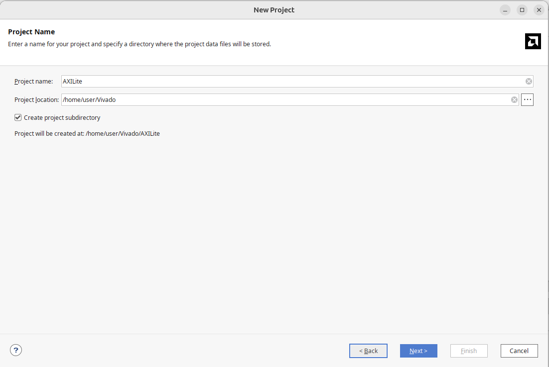
- Create Project to specify Project Name and Locations
- Project Type specify as RTL Project
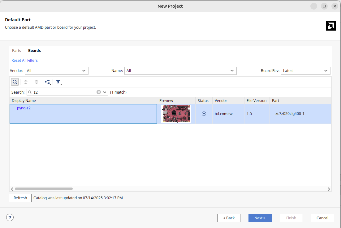
- Default Parts select installed pynq-z2 in Boards
This will create a blank project.
Creating AXI Lite Slave IP
In Zynq architecture, one of the most common control interfaces is AXI Lite, which is suitable for the most basic IP CSR writing and reading. Our example here is a very simple module:
- reg0: input 32 bits integer A
- reg1: input 32 bits integer B
- reg2: output 32 bits integer C = A + B
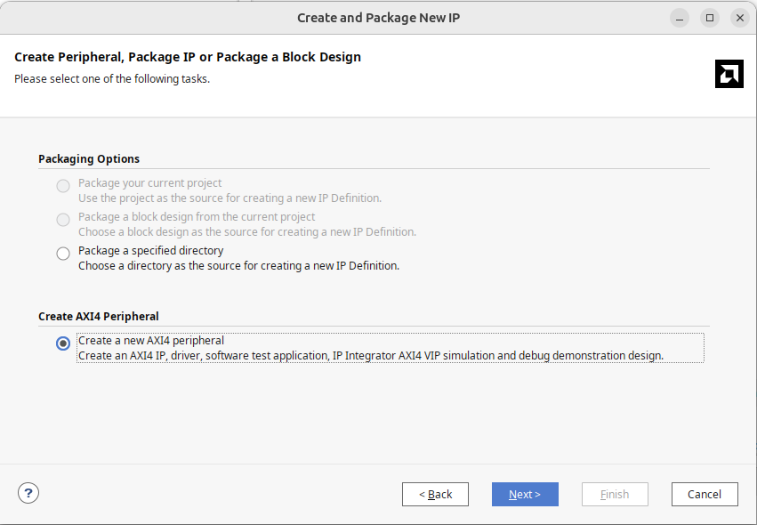
To create an AXI4-Lite Slave IP in Vivado, the process is as follows:
- Tools -> Create and Package New IP
- Select Create a new AXI4 Peripheral
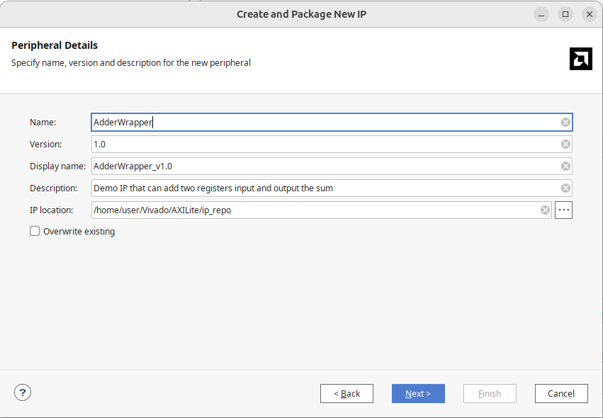
- Peripheral Detail fill in the module's information; here, let's call this module AdderWrapper
- Add Interfaces remain as is, one AXI Lite mode choose Slave, set the number of Registers to 4, if the design is large, this can be set up to 512 registers.
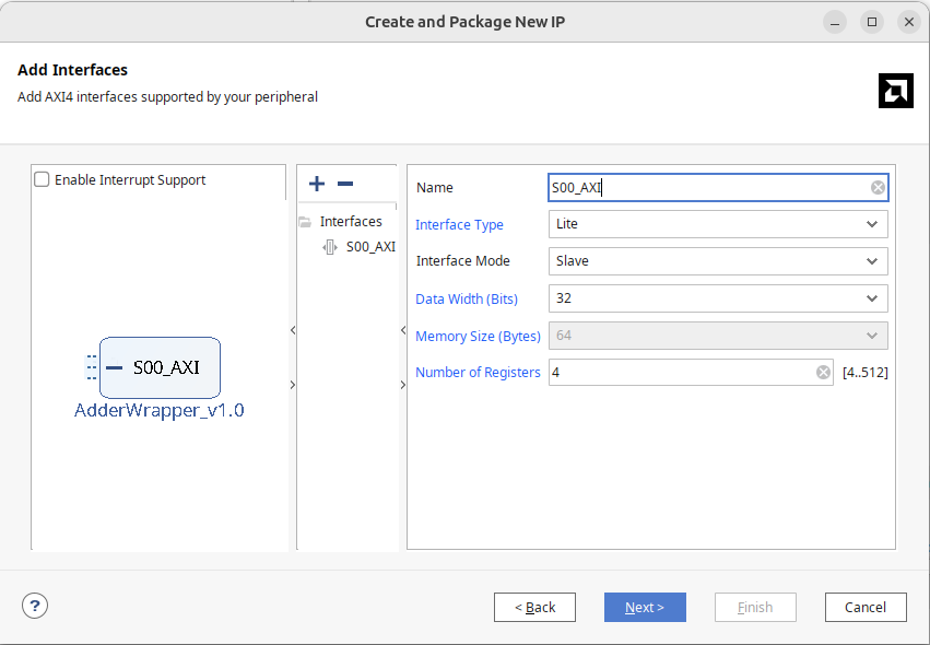
- Create Peripheral can choose to Add IP to the repository to first connect block design; or choose Edit IP to edit IP.
Editing AXI Lite IP
After opening AdderWrapper, you can see the Vivado-generated code
- The top level AdderWrapper.v
- The lower-level AXILite Handler: AdderWrapper_slave_lite_v1_0_S00_AXI.v, hereafter referred to as S00_AXI.v.
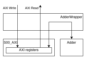
Vivado's design logic is like this:
AdderWrapper provides an AXI Lite interface, which channels the entire signal into AXILite Handler, accessing AXI Lite registers within.
S00_AXI.v is an AXI interface implementation, besides more parameters, it's still understandable. It’s recommended to familiarize oneself with the AXI protocol through this module. Simply put, AXI consists of five independent channels: AW, AR, W, R, B, each channel is controlled by valid/ready, transferring corresponding data. During writing, the AW channel transfers the writing address, storing in the axi_awaddr variable; the W channel writes data into slv_reg; the B channel returns the writing result. During reading, the AR channel transfers the reading address, storing in the axi_araddr variable; the R channel returns the read content axi_rdata and reg_data_out.
Though not explicitly stated, the modifications here will be:
- Connect your module Adder.v inside AdderWapper.v
- Declare all connecting lines as wire in AdderWrapper.v, and become S00_AXI.v's port
- In S00_AXI.v, connect these lines to the registers provided by S00_AXI.v
Drawn in a diagram, it would look like this:
The content of Adder.sv is as follows:
module Adder (
  input [31:0] a,
  input [31:0] b,
  output [31:0] c
);
assign c = a + b;

endmodule
Additional methods include:
- File -> Add Sources -> Add or create design sources -> Select Adder.sv
- Declare three lines a, b, c each with a width of 32 bits
- Instantiate Adder.sv inside AdderWrapper.sv
- Declare a, b, c ports at S00_AXI.v interface, note the port direction is opposite to Adder.sv, as inputs to Adder.sv are stored in registers in S00_AXI.v, so in S00_AXI.v, it will be output port.
- In S00_AXI.v, assign slv_reg0, slv_reg1 to a, b; write c to reg_data_out when reading offset 2.
Finally, click Edit Packaged IP on the left side, continue to the end, and press Re-Package IP to complete IP packaging.
Connecting Block Diagram
1 Create Zynq Processing System
Choose Vivado's Create Block Design, generally naming Design as design_1.
- In Block Diagram, use Add IP to add ZYNQ7 Processing System
- Use Run Block Automation, let Vivado automatically complete DDR and FIXED_IO
If Run Block Automation appears, it's almost as a standard procedure, let Vivado handle it.
2 Add Custom AXI Lite IP
Find your AdderWrapper in the IP list and add it to the Block Diagram, again using Run Block Automation, Vivado will automatically call up AXI Interconnect and Reset modules. The AXI Interconnect is the switch of the AXI bus, capable of connecting multiple masters and slaves, and it manages arbitration, address decoding, and other tasks. Here, a 1 master 1 slave AXI Interconnect is sufficient.
3 Wrap Up
Once completed, the entire Block Diagram typically includes:
- Zynq PS
- AXI Interconnect
- Custom AXI Lite IP
- Clock / Reset Modules
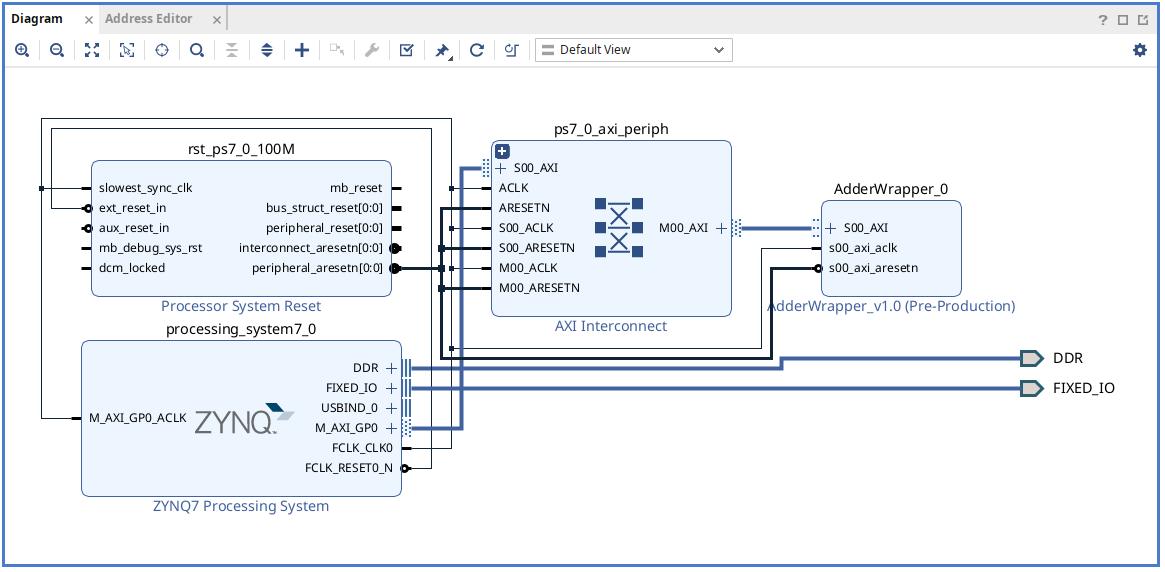
At this point, the PS can already access your designed hardware module through AXI Lite, the last step is to right-click on design.bd at the project hierarchy, select Create HDL Wrapper, this wrapper file will include all the modules you've designed and their Verilog code. In the later AXI Stream section, we'll encounter situations where we need to inspect this file to successfully troubleshoot, but generally unless there's an exception, you don't need to inspect the generated "trash" Verilog code.
Testing on Board
Generating bitstream
After designing, the next step is to run it on the board. Similar to chip burning, Vivado will go through the following steps:
- Synthesis: Converting the RTL into logic gates and registers, the synthesis target on FPGA will be basic elements such as LUT (Look-up table) and FF (flip flop).
- Implementation: Laying out the synthesis results onto the selected FPGA model.
- Generate Bitstream: Writing the layout results into a bitstream file for burning onto the FPGA
Once Generate bitstream is completed, two files are needed:
- .bit file, under
<Project Name>.runs/impl_1/, this is the bitstream file to be burned into the FPGA - .hwh file, hwh stands for hardware handoff file, it tells the Zynq PS system how to communicate with this hardware, under
<Project Name>.gen/sources_1/bd/design_1/hw_handoff/
Since it's very troublesome, I usually find them by searching for file extensions .bit or .hwh. The two file names are usually different, one is the block diagram .bd name, the other is the HDL wrapper name, first rename them to the same name, hereafter referred to as AdderWrapper.bit and AdderWrapper.hwh.
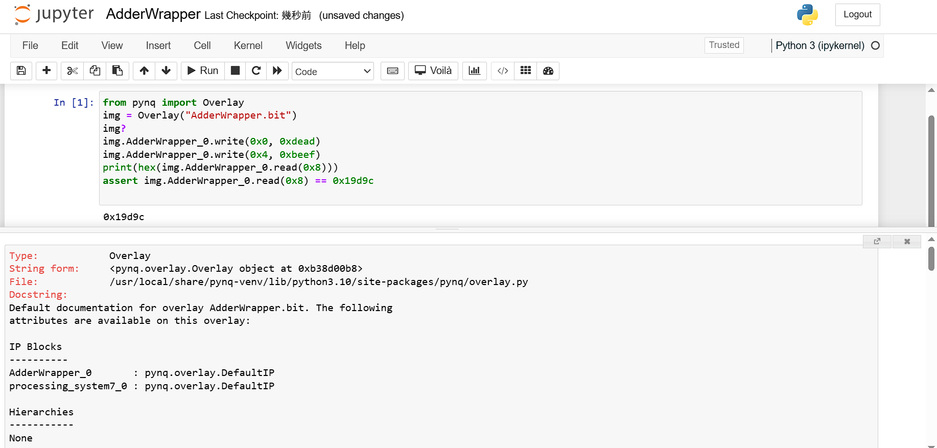
Jupyter Notebook Testing
Upload .bit and .hwh to the jupyter notebook, open a new python3 file.
Below are the python code and screenshot during operations, the implementations of pynq and Overlay are packages provided by Xilinx allowing dynamic loading of the .bit file you want to test. Since we place the A, B, C of the Adder module in registers 0, 1, 2, corresponding to AXI addresses 0x0, 0x4, and 0x8.
from pynq import Overlay
img = Overlay("AdderWrapper.bit")
img?
img.AdderWrapper_0.write(0x0, 0xdead)
img.AdderWrapper_0.write(0x4, 0xbeef)
print(hex(img.AdderWrapper_0.read(0x8)))
assert img.AdderWrapper_0.read(0x8) == 0x19d9c
Conclusion
Pynq-Z2 is an entry-level development board with the Zynq architecture. Using Vivado and AXI Lite, you can build an SoC FPGA, quickly loading different IPs for testing and verification on the software side.
After finishing AXI lite, in the next chapter, we'll first return to the lower-level AHB bus, to see how to configure different interfaces in the IP and connect them with ports in verilog.