This content is translated with AI. Please refer to the original Traditional Chinese version (zh-TW) for accuracy.
When going online and offline, the parts that require time to operate are mainly floorplan and powerplan. Once placement has started, it's about pressing a button and then watching animations, coming back after watching a segment to see if it's finished.
For example, during a recent offline session, I watched the entire season of MYGO . During the previous 1P3M , I watched the entire season of Frieren.
Overall, the steps here are repeated as follows:
- Report Timing and wait for the result.
- If there is a timing violation in the result, run ECO and wait for the result.
- Repeat ECO until the Report Timing is fine, then proceed to the next step.
In general, these are to be done:
- Placement
- Analyze Pre-CTS setup time
- CTS
- Analyze Post CTS setup time
- Analyze Post CTS hold time
- Insert TieHi, TieLo cells
- Route
- Analyze Post Route setup time
- Analyze Post Route hold time
- Use tempus to analyze Signoff setup time
- Tempus analyzes Signoff hold time
- Use a tool for Signoff ECO
Depending on the size of your design, each step is a combination of clicking a button + watching animation + saving, you can even take a nap, simply put:

There are several noteworthy points in this entire process:
- Don't worry about DRC. Although DRC is run during Floorplan, once placement starts, a large number of DRC errors will emerge, which will only be resolved after Route.
- Don't backtrack: once CTS is done, don't run Pre-CTS Analysis; once Route is done, don't run Post-CTS's ECO, as INNOVUS will directly crash; please close INNOVUS and reload the file.
- Furthermore, please remember to save your files. If it is for work purposes, you can develop the habit of screenshotting and saving the results of Timing Reports and Placement Reports, as the final report before going offline will use them.
Placement
In the placement stage, standard cells are placed onto the Follow Pins drawn in the previous step. INNOVUS introduced a feature called early clock flow (EOF), which was later adopted by Synopsys ICC2. Here's the story: In the past, standard cells were placed during placement, and the clock tree grew during CTS. The problem was that placement occupied all available space, so Clock Tree cells found no space when they came in, and the clock tree didn't grow well if placed far away. Instead of this, it's better to perform some CTS during placement. Though it takes more time, it prevents Timothy issues during CTS that require ECO solutions.
The implication of this is that the density after placement will spike and actually decrease after CTS, which is a point that will be questioned in reports.
The placement setting placement.tcl is as follows (including early_clock_flow):
set_db design_process_node 90
set_db timing_analysis_type ocv
set_db timing_analysis_cppr both
set_db design_early_clock_flow true
create_basic_path_groups -expanded
Execute
source placement.tcl
place_opt_design
CTS
The full name of CTS is Clock Tree Synthesis, which synthesizes clock signals. A major hardware implementation assumption is that the clock will simultaneously reach all registers on the chip, and CTS is the tool that achieves this as much as possible.
CTS determines chip quality because the main source of chip power consumption is signal switching, with the clock being the largest source (changing frequency 50%, thank you), accounting for about 30% of total chip power. Meanwhile, the Cells used in CTS, whether Buffer or Inverter, are specially designed cells to shorten transition time and balance rising/falling time, making CTS's overall area occupy about 10% of the chip.
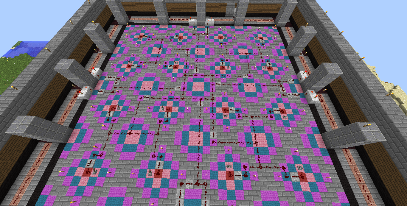
To understand the technology behind it, you can study H-tree, which I once used early in my Minecraft farm building. Here's a previous old image:
H-tree splits the chip into two blocks and gradually subdivides them, but INNOVUS seems to divide them into three blocks, an improved version of the H-tree. However, this is a bit too detailed, and as long as CTS is good, who cares what tree you used.
After finishing CTS, several indicators are produced:
- Clock latency: how long the clock takes to reach the register
- Clock transition time: how long it takes for the clock to go from 0 to 1
- Clock skew: since reaching each register at exactly the same time is impossible, what is the time difference between the fastest and slowest
The quality of Transition time and skew affects subsequent STA analysis. As you can imagine, the larger the skew, the more different the clock times received by two registers, compressing the cycle between them, making setup time harder to satisfy. Clock Latency and transition time settings affect CTS synthesis. If you demand extreme transition time, then use the biggest and fastest buffer on the CTS path, increasing power consumption and area. Conversely, if transition time is too long, the clock cycle will compress, causing timing issues.
CTS Settings
INNOVUS divides the CTS structure into three parts like a tree: ‘Top’, ‘Trunk’, ‘Leaf’. From rough to fine, to ensure clock signal purity and avoid interference from surrounding circuits, the following measures can be used:
- Keep CTS wire a bit farther from others (spacing)
- Make CTS wire thicker (width)
- Clamp it like padding with ground on both sides
Relevant settings are as follows:
# Please modify cell names according to your process
set_db cts_buffer_cells {CLKBUF*}
set_db cts_inverter_cells {CLKINV*}
set_db cts_clock_gating_cells {CLKGATE*}

set_db cts_update_clock_latency false

set_db cts_target_max_transition_time_trunk 150ps
set_db cts_target_max_transition_time_leaf 100ps
set_db cts_target_skew 100ps

create_route_rule -name cts_2w2s \
  -spacing_multiplier {metal3:metal6 2} \
  -width_multiplier {metal3:metal6 2} \
  -generate_via
create_route_rule -name cts_2s
  -spacing_multiplier {metal3:metal6 2} \

create_route_type -name cts_leaf \
  -top_preferred_layer metal4 \
  -bottom_preferred_layer metal3 \
  -route_rule cts_2s
create_route_type -name cts_trunk \
  -top_preferred_layer metal6 \
  -bottom_preferred_layer metal5 \
  -route_rule cts_2w2s
create_route_type -name cts_top \
  -top_preferred_layer metal6 \
  -bottom_preferred_layer metal5 \
  -route_rule cts_2w2s

set_db cts_route_type_top cts_top
set_db cts_route_type_trunk cts_trunk
set_db cts_route_type_leaf cts_leaf
set_db cts_top_fanout_threshold 1000
I don't think much explanation is needed. Execute CTS:
source cts_setup.tcl
create_clock_tree_spec
ccopt_design
CTS Debugging
To balance the overall CTS, use:
Clock->CCOpt Clock Tree Debugger- In Debugger,
View->Enable clock path browserto inspect.
As the frequency pushes towards the design limit, INNOVUS will adjust CTS, allocating more time to more time-consuming paths using the useful skew mechanism. In the Clock path browser, one will gradually see the clock tree become unbalanced, and skew increase.
While executing CTS, INNOVUS uses the largest CLKBUF's max_transition to calculate. In other words, that's the smallest transition the largest CLKBUF can achieve. If you set it smaller naturally, you won't reach it. Errors encountered are:
IMPCCOPT-1209 Non-leaf slew time target of 0.150ns is too low
IMPCCOPT-1013 The target_max_trans is too low for at least one clock tree, net type and timing corner
Look upwards to find warning messages like:
Slew time target (leaf, trunk, top} 0.100ns (Too low; min: 0.500ns)
At this point, obediently set it to 500ps or change to another process.
How to run ECO
After completing a step, first analyze Timing
Timing->Report Timing- In Design Stage, choose according to the current stage, with
Pre CTS,Post CTS,Post Route,Signoffbeing the four stages to pass - For Analysis Type, choose
SetupandHoldsequentially, because Pre CTS does not yet have Clock Tree, so there's no Hold to analyzepass four levels and defeat seven foes
After execution, check the terminal for any Timing violations. If there are, begin running ECO.
ECO->Optimize Design- In Design Stage, choose according to the current stage, remembering not to rerun past stages
- For Optimization Type, choose
SetuporHold. In fact, both can be run simultaneously, though I've never tried - Incremental and full ECO by choosing Setup/Hold are mutually exclusive, refer to the following
- In Design Rules Violations, select
Max Cap,Max Tran,Max Fanoutif violated
Since ECO Timing Violation is prioritized, its background order of observation is:
- Fix Timing
- Fix DRVs
- If Timing breaks again, fix Timing
The existence of the third step sometimes results in unrepairable DRVs. A peculiar little trick here is not to keep running Setup/Hold but alternate between running full ECO and Incremental ECO, unexpectedly making it easier to fix Timing Violation and DRVs together.
Route
By this point, there's nothing much to say; proceed to actual operation. The first step is to insert Tie High / Tie Low cell:
Place->Tie HI/LO->Add- In
Select, choose High Low cells - In
Mode, parameters for insertion can be set; common reference values aremax_distance100 andmax_fanout16, but I generally choose not to set them
Start Routing
Route->NanoRoute->Route- Check
Optimize ViaandOptimize Wire - For End Iteration, choose
default - Check
Fix Antenna,Insert Diodes; fill in Diode Cell name with the process-provided ANTENNA cell - Check
Timing Driven,SI Driven
Click OK, and you can go to sleep. This takes a while; when finished, zoom in to check the details, see how the points are connected—even though it's delicate and complex, there's a peculiar beauty.
During Route, INNOVUS will tie up loose ends and resolve DRC errors. If your layout still has errors after Route completion, inspect whether there's a need for Floorplan correction. For example, as mentioned several times: a black box without placement halo, its power ring M2 covering standard cells, which is unsolvable no matter how you route, will show DRC errors after Route.
Final Wrap-up Output
Normally here a dynamic power analysis with a waveform file would be done, but we can skip that for now.
After completing signoff timing check, some final touches remain:
Insert Filler Cell
Filler cells are dummy cells inserted in the gaps between standard cells
Place->Physical Cells->Add Filler- In
Select, choose all Cell widths from X1, X2 … X64 - OK to insert Filler Cells
Insert Dummy Metal
Dummy Metal ensures the metal layer's density meets process limits. This step can be confirmed with the upper integration unit, and it might not necessarily be done here:
Route->Metal Fill->Setup- Set each metal layer’s target
Max Metal Density, the DRC limit is usually 70, generally setting it to 40-50 is sufficient Route->Metal Fill->Add- Uncheck Tie High/Low to net(s); in Timing Aware, select
Critical net from Timing Analysis, enterSlack Thresholdfrom 0.1 to 0.2 - OK to insert Metal Fill
Adding dummy metal should increase capacitance between metals, affecting timing, but INNOVUS will ensure (or at least you believe) that the effect doesn’t exceed the slack value.
Final Check
Three checks should run without errors:
Check->Check DRCCheck->Check Connectivity, uncheckDanglingWire (Antenna)Check->Check Process Antenna
Export .sdf
Proceed directly, execute the following script
# write_sdf.tcl
# source write_sdf.tcl
write_sdf CHIP.sdf \
  -max_view AV_func_max \
  -typical_view AV_func_max \
  -min_view AV_func_min \
  -map_removal -recompute_delaycal
write_netlist CHIP.v
write_netlist -include_pg_ports CHIP_pg.v
Among them, CHIP.sdf and CHIP.v are used for post-layout simulation. CHIP_pg.v includes power/ground pins, used for LVS.
Export .gds
Here a streamOut.map is used, responsible for translating INNOVUS layers to gds layers. I've written this file before, but it's lost now… so let's skip. Standardcel.gds and hardmacro.gds should be provided by the PDK and hard macro vendor.
# write_stream.tcl
write_stream CHIP.gds -map_file streamOut.map -lib_name DesignLib \
  -merge { \
    standardcell.gds \
    pad.gds \
    hardmacro.gds \
  } \
  -uniquify_cell_names -unit 2000 -mode all
CHIP.gds is the final layout for tapeout. Before sending out, go through the last signoff step, referring to the previously published Signoff Chapter .