This content is translated with AI. Please refer to the original Traditional Chinese version (zh-TW) for accuracy.
Finally entered Power Plan, this part is like wiring your house, from the power supply pad all the way to the lowest level standard cell. You need to complete Power Ring, Macro Ring, Power Stripe, and Follow Pin.
Power Ring
Generally, the Power Pad will supply power from layers M1-M3, so the Power Ring usually stops at M4 or M5 to avoid blocking the lines coming from the Pad. I generally choose a width of 3-4 um for the Power Ring, depending on the power consumption and number of Wire Groups of the chip. The metal process has a density limit, generally between 30% - 70%. The width of the gap in the Power Ring is set to half the line width. This gives an overall metal density of 66%, which is just within the upper limit of the density check of 70%.
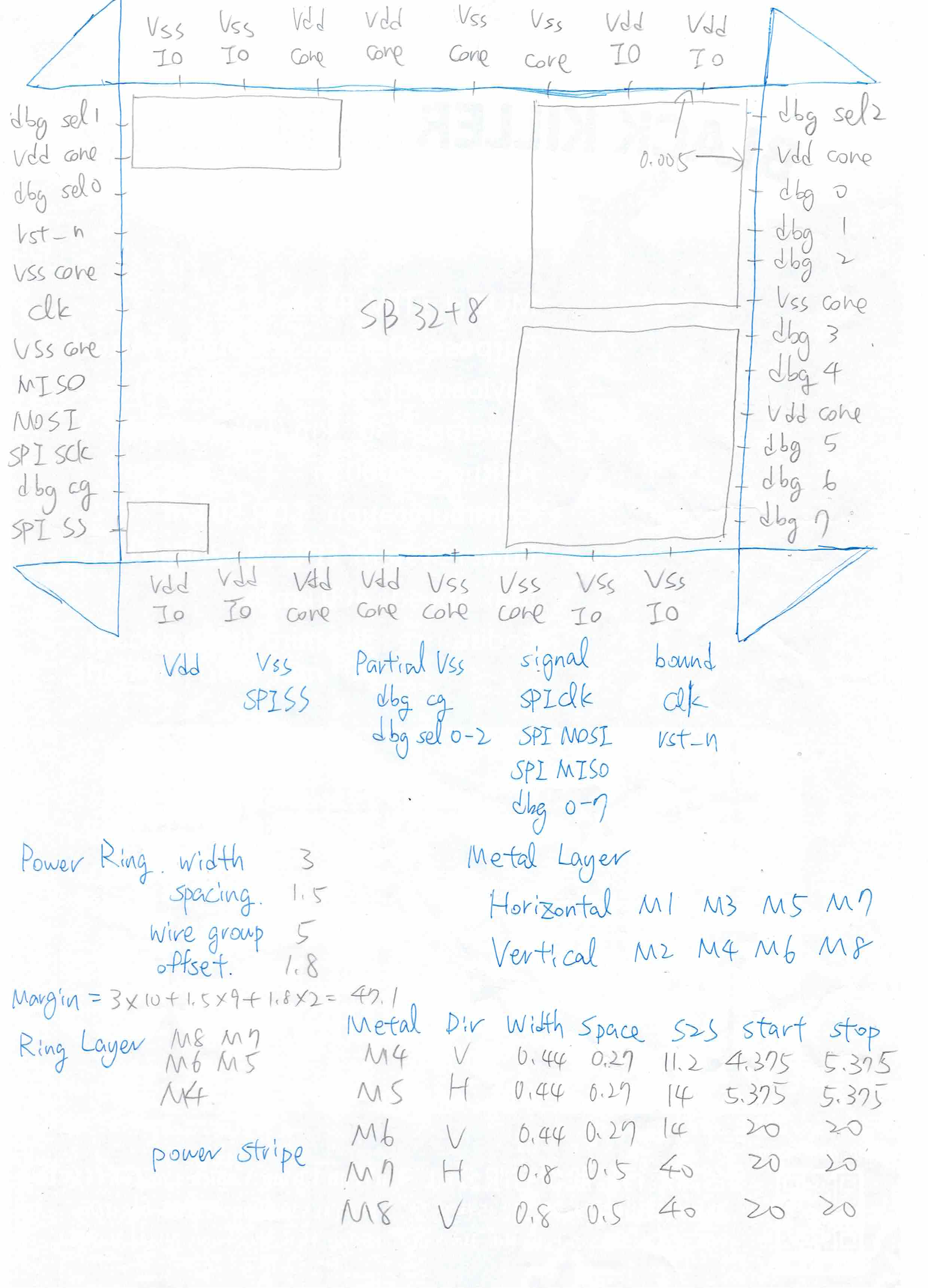
In my previous implementation, the Power Ring width was 3, the spacing was 1.5, using 3 Wire Groups, with a distance of 1.8 between the chip Core and Power Pad. Then, when setting the Floorplan, the setting for Core to IO Boundary needs to be increased by: $3 \times 6 + 1.5 \times 5 + 1.8 \times 2 = 29.1 $ Rounded to an integer, you choose 30, a commonly used number, so write it down on A4.
Actual Operation
Power->Power Planning->Add Ring- Fill in
VDD VSSfor the Net - Sequentially add Power Ring from top to bottom, setting Top and Bottom as horizontal metal layers; Left and Right as vertical metal layers.
- In
Advanced page, checkWire groupandInterleaving, and fill in the number of Wire Group sets.
With the Power Ring, you can now connect the Power Pad:
Route->Special Route- Fill in
VDD VSSfor Net(s) - Select
Pad pinsfor SRoute - Set
Number of Connections to Multiple Geometriesto All in the Pad Pins item ofAdvanced Page - On the
Via Generationpage, selectCore RingforMake Via Connections To
Macro Power
Generally, Macro has the following power supply methods:
Power Ring
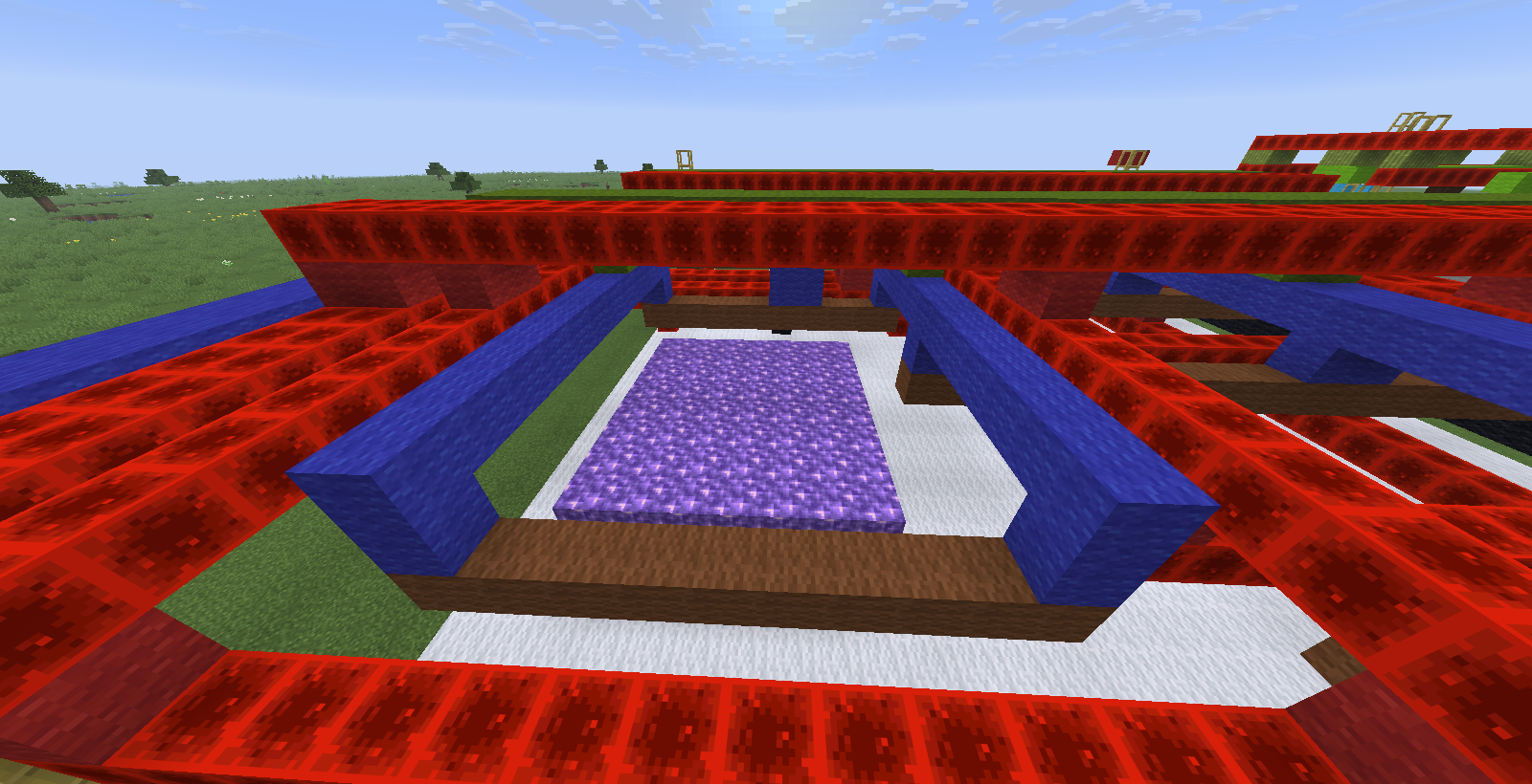
This type of black box comes with two circles of Power Ring outside, for VDD and VSS respectively, usually with vertical on M2 and horizontal on M3. This is the simplest power supply; setting a vertical M4 Power Stripe over the black box will have INNOVUS automatically connect M4 to the horizontal M3.
Just like building in Minecraft, from left and right respectively, the inner circles of blue and brown and outer red Macro Ring are on M2 M3 of VSS VDD; we directly cover them with green M4 Power Stripe to complete the power supply.
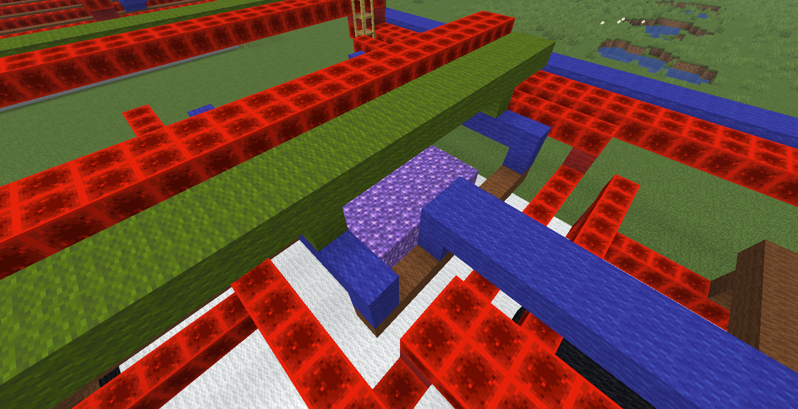
Power Rail
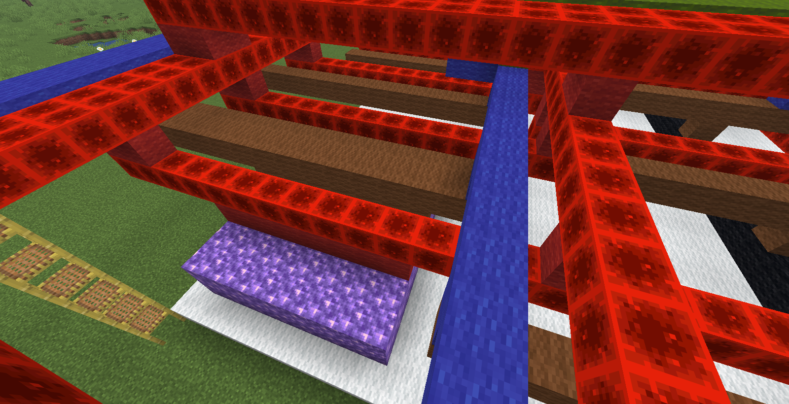
Power Rail refers to strips of metal on the top layer of the black box, interleaving VDD and VSS, usually as vertical pins on the layout, such as M4. The connection method is called Over P/G pin, which will connect strips of M4 above to VDD/VSS. To prevent the Power Stripe from extending beyond the black box, a Macro Ring is added (this explains why the black box should be placed at the corners).
As shown below, blue M3 and brown M2 are the Macro Ring, while the central red, brown, and red stripes are P/G pins, with P/G pins coming out from M2 blocked by the M3 Macro Ring.
Power Pin
Power Pin refers to contact points of VDD/VSS on the black box, which can be routed out using INNOVUS special route (Route -> SRoute); like Power Rail, it requires adding a Macro Ring to block the wires. I haven't encountered this, so I won't draw it.
Actual operation
Adding a Macro Ring is the same as adding a Core Ring:
Power->Power Planning->Add Ring- Choose
Block ring(s) aroundfor Ring Type, andEach selected block and/or group of core rows - Specify the shape to be added in the
Advanced Page
For the Over P/G Pin type:
Power->Power Planning->Add Stripes- Fill in
VDD VSSfor Net - Select
Over P/G pinsinSet Pattern - In the
ModePage, selectRingforExtend to closest target; setTop stack via layerto the layer above the Macro Ring
This will add P/G pin stripes.
Power Stripe
It is recommended to do Power Stripe above M4, leaving M2 and M3 for Routing. The two large and thick Power Stripes severely interfere with Routing lines, especially when there are few metal layers . Therefore, in the case of 1P3M, I sparsely place the Stripe in M3.
The place new chip designers are most puzzled over, the biggest question is so how do I set my width and distance...? The answer is: I don't know One time I reduced the M4 width from 0.44 to 0.40, and in the end, every via connecting M4 to M1 reported a DRC error, and I had to redo the Floorplan altogether.
Below are some values I previously used in practice, whose origins are unknown but which work. You can make slight adjustments based on your power consumption and process DRC.
| Metal Layer | Direction | Width | Space | Set to Set | Start | Stop |
|---|---|---|---|---|---|---|
| M4 | Vertical | 0.44 | 0.27 | 11.2 | 4.375 | 5.375 |
| M5 | Horizontal | 0.44 | 0.27 | 14 | 5.375 | 5.375 |
| M6 | Vertical | 0.44 | 0.27 | 14 | 20 | 20 |
| M7 | Horizontal | 0.8 | 0.5 | 40 | 20 | 20 |
| M8 | Vertical | 0.8 | 0.5 | 40 | 20 | 20 |
This table is extremely important and also documented on my Layout A4, with rows and columns marked with pen and values with a pencil. In my experience, due to avoiding some Macros or Power Pads, start/stop is the most frequently changed part, thus the 4.375 number previously discussed is odd out.
Actual Operation
Power->Power Planning->Add Stripes- Fill in
VDD VSSfor Net - Set parameters
LayerSets-to-set distanceWidthSpacingStartStop - Set
Top stack via layerto the layer above in theMode Page,Bottom stack via layerto the layer below. For instance, when adding M5 Stripe, set Top to M6 and Bottom to M4. - Uncheck
Pad/Core ring connectionBlock ring connectionfor Allow Jogging
Follow Pin
The height and width of Follow Pin are pre-set, so there is nothing much to mention:
Actual operation
Route->Special Route- Fill in
VDD VSSfor Net(s) - Select
Follow pinsfor SRoute; uncheckAllow joggingunderLayer Change Control - On the
Via Generationpage, select the lowest Power Stripe forTop Stack Via Layer, this time it is M4 - On the
Via Generationpage, selectCore RingStripeBlock RingBlock PinforMake Via Connections To
Following the previously mentioned A4 page, the bottom half is prepared for Power Plan. Please remember there are many places for changes, so recording must use a pencil. This page mixes pin information from one run and process data from another, with pencil-filling indicating parts that might change, and pen indicating parts that largely won't change.
DRC check
Normally at this point, one should run Rail Analysis for power analysis, but this part requires its own article, and we'll skip it for now.
After completing FloorPlan, conduct a DRC and connectivity check once.
Connectivity Check
- Select
Check->Check Connectivity - Choose
Special Onlyfor Net Type - Choose
Namedfor Net and fill inVDD VSS - Uncheck
Dangling Wire (Antenna)
Check if there are violations; if so, there is a short circuit in VDD/VSS.
INNOVUS DRC Check
Check -> Check DRC, correct the relevant errors. In FloorPlan, PowerPlan, some common error-prone areas include:
- The place in Power Stripe and Power Pad where Pad Pins are drawn, in the overlapping area with Power Ring.
- Similarly, in the overlapping area of Follow Pin and Pad Pin, briefly, Pad Pin is the root of all evils.
- In the overlapping area of P/G pin and Power Stripe on Macro Ring
Such as Via too close (Cut_Spacing), Via overlapping (Cut_Short), or two rows of metal too close (parallel run length spacing), and so on.
Calibre DRC Check
Because INNOVUS’s check is designed for speed, letting the tool quickly know whether there is a problem with the design, its rules and checking mechanism are not as complete.
Please refer to the Signoff section to export the .gds file and use Calibre and other DRC tools for checking and fixing all DRC errors.
Extended Content and Conclusion
Due to limited space and to stick to the topic, parts of the content are omitted; these mainly include:
The first is how to use Blockage assistance and DRC debugging. If fully implementing the steps mentioned above, the DRC Check will surely be super painful, spewing out many of the errors mentioned earlier.
Regarding Pad Pins, an easy way is to place Blockage directly at the Pad Pin positions, preventing Power Stripe and Follow Pin from extending into Power Ring and Pad Pin overlap, thus easily avoiding many errors. Macro Ring operations on Via have some techniques that can quickly deal with DRC Errors, but you can't find these methods online, and I'm unable to write how to operate without INNOVUS at hand.
The second is about Power Analysis.
After finishing PowerPlan, theoretically, you should use INNOVUS's integrated Voltus for Power Analysis and IR Drop Analysis to ensure the Power Ring and Power Stripe adequately support the current required by the chip core without causing significant voltage drops. It's much like really building a house; after wiring, check if the wire is thick enough. If not, prepare for a house fire. Writing about this would be enough to fill a chapter, and I haven't fully learned it myself yet, mostly applying the settings made by others, so let's skip for now.
After solving all DRC errors, the chip's FloorPlan/PowerPlan is complete; save the file, preparing to proceed to P&R, where upcoming operations will be comparatively monotonous.